- 您现在的位置:买卖IC网 > PDF目录10137 > AD7710ARZ-REEL (Analog Devices Inc)IC ADC 24BIT DIFF INP 24-SOIC PDF资料下载
参数资料
| 型号: | AD7710ARZ-REEL |
| 厂商: | Analog Devices Inc |
| 文件页数: | 7/32页 |
| 文件大小: | 0K |
| 描述: | IC ADC 24BIT DIFF INP 24-SOIC |
| 标准包装: | 1,000 |
| 位数: | 24 |
| 采样率(每秒): | 1.03k |
| 数据接口: | 串行 |
| 转换器数目: | 1 |
| 功率耗散(最大): | 45mW |
| 电压电源: | 模拟和数字,双 ± |
| 工作温度: | -40°C ~ 85°C |
| 安装类型: | 表面贴装 |
| 封装/外壳: | 24-SOIC(0.295",7.50mm 宽) |
| 供应商设备封装: | 24-SOIC W |
| 包装: | 带卷 (TR) |
| 输入数目和类型: | 2 个差分,单极;2 个差分,双极 |
第1页第2页第3页第4页第5页第6页当前第7页第8页第9页第10页第11页第12页第13页第14页第15页第16页第17页第18页第19页第20页第21页第22页第23页第24页第25页第26页第27页第28页第29页第30页第31页第32页
AD7710
REV. G
–15–
Antialias Considerations
The digital filter does not provide any rejection at integer mul-
tiples of the modulator sample frequency (n
× 19.5 kHz, where
n = 1, 2, 3 . . . ). This means that there are frequency bands
±f
3 dB wide (f3 dB is cutoff frequency selected by FS0 to FS11),
where noise passes unattenuated to the output. However, due to
the AD7710’s high oversampling ratio, these bands occupy only
a small fraction of the spectrum, and most broadband noise is
filtered. In any case, because of the high oversampling ratio a
simple RC, single-pole filter is generally sufficient to attenuate
the signals in these bands on the analog input and thus provide
adequate antialiasing filtering.
If passive components are placed in front of the AD7710, ensure
that the source impedance is low enough to keep from intro-
ducing gain errors in the system. The dc input impedance for
the AD7710 is over 1 G
. The input appears as a dynamic
load that varies with the clock frequency and with the selected
gain (see Figure 7). The input sample rate, as shown in Table III,
determines the time allowed for the analog input capacitor CIN
to be charged. External impedances result in a longer charge
time for this capacitor, which may result in gain errors being
introduced on the analog inputs. Table IV shows the allowable
external resistance/capacitance values that do not introduce gain
error to the 16-bit level, while Table V shows the allowable
external resistance/capacitance values that do not introduce gain
error to the 20-bit level. Both inputs of the differential input
channels look into similar input circuitry.
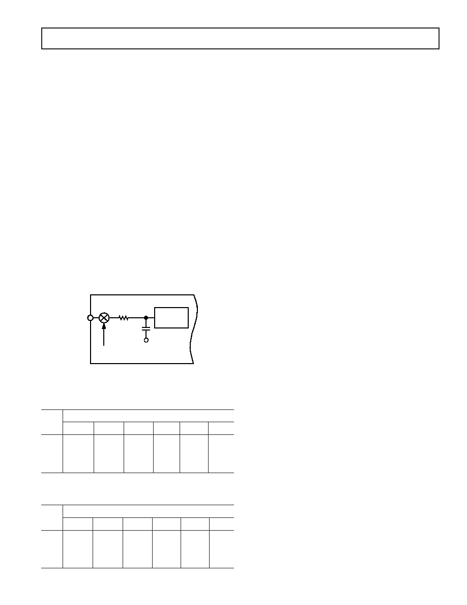
RINT
7k
TYP
CINT
11.5pF TYP
VBIAS
AIN
SWITCHING FREQUENCY DEPENDS ON
fCLKIN AND SELECTED GAIN
HIGH
IMPEDANCE
>1G
AD7710
Figure 7. Analog Input Impedance
Table IV. External Series Resistance That Do Not Introduce
16-Bit Gain Error
External Capacitance (pF)
Gain
0
50
100
500
1000
5000
1
184 k
45.3 k 27.1 k 7.3 k 4.1 k 1.1 k
2
88.6 k
22.1 k 13.2 k 3.6 k 2.0 k 560
4
41.4 k
10.6 k 6.3 k
1.7 k
970
270
8–128
17.6 k
4.8 k
2.9 k
790
440
120
Table V. External Series Resistance That Do Not Introduce
20-Bit Gain Error
External Capacitance (pF)
Gain
0
50
100
500
1000
5000
1
145 k
34.5 k 20.4 k 5.2 k 2.8 k 700
2
70.5 k
16.9 k 10 k
2.5 k
1.4 k 350
4
31.8 k
8.0 k
4.8 k
1.2 k
670
170
8–128
13.4 k
3.6 k
2.2 k
550
300
80
The numbers in Tables IV and V assume a full-scale change on
the analog input. In any case, an error introduced due to longer
charging times is a gain error that can be removed using the
system calibration capabilities of the AD7710, provided that the
resultant span is within the span limits of the system calibration
techniques.
ANALOG INPUT FUNCTIONS
Analog Input Ranges
Both analog inputs are differential, programmable gain input
channels that can handle either unipolar or bipolar input signals.
The common-mode range of these inputs is from VSS to AVDD,
provided that the absolute value of the analog input voltage lies
between VSS –30 mV and AVDD +30 mV.
The dc input leakage current is 10 pA maximum at 25
°C
(
±1 nA over temperature). This results in a dc offset voltage
developed across the source impedance. However, this dc offset
effect can be compensated for by a combination of the differen-
tial input capability of the part and its system calibration mode.
Burnout Current
The AIN1(+) input of the AD7710 contains a 4.5
A current
source that can be turned on/off via the control register. This
current source can be used in checking that a transducer has not
burned out or gone open circuit before attempting to take mea-
surements on that channel. If the current is turned on and
allowed to flow into the transducer and a measurement of the
input voltage on the AIN1 input is taken, it can indicate that the
transducer has burned out or gone open circuit. For normal
operation, this burnout current is turned off by writing a 0 to
the BO bit in the control register.
Output Compensation Current
The AD7710 also contains a feature that allows the user to
implement cold junction compensation in thermocouple appli-
cations. This can be achieved using the output compensation
current from the IOUT pin of the device. Once again, this current
can be turned on/off via the control register. Writing a 1 to the
IO bit of the control register enables this compensation current.
The compensation current provides a 20
A constant current
source that can be used in association with a thermistor or a
diode to provide cold junction compensation. A common
method of generating cold junction compensation is to use a
temperature dependent current flowing through a fixed resistor
to provide a voltage that is equal to the voltage developed across
the cold junction at any temperature in the expected ambient
range. In this case, the temperature coefficient of the compensa-
tion current is so low compared with the temperature coefficient
of the thermistor that it can be considered constant with tem-
perature. The temperature variation is then provided by the
variation of the thermistor’s resistance with temperature.
Normally, the cold junction compensation will be implemented
by applying the compensation voltage to the second input chan-
nel of the AD7710. Periodic conversion of this channel gives the
user a voltage that corresponds to the cold junction compensa-
tion voltage. This can be used to implement cold junction com-
pensation in software with the result from the thermocouple
input being adjusted according to the result in the compensation
channel. Alternatively, the voltage can be subtracted from the
input voltage in an analog fashion, thereby using only one chan-
nel of the AD7710.
相关PDF资料 |
PDF描述 |
|---|---|
| VE-BNJ-MW-F2 | CONVERTER MOD DC/DC 36V 100W |
| VI-22M-IW-F3 | CONVERTER MOD DC/DC 10V 100W |
| VE-B4R-MY | CONVERTER MOD DC/DC 7.5V 50W |
| LTC2852HS#TRPBF | IC TXRX RS485/RS422 14SOIC |
| MS3102A24-12PX | CONN RCPT 5POS BOX MNT W/PINS |
相关代理商/技术参数 |
参数描述 |
|---|---|
| AD7710ARZ-REEL7 | 功能描述:IC ADC 24BIT DIFF INP 24SOIC RoHS:是 类别:集成电路 (IC) >> 数据采集 - 模数转换器 系列:- 标准包装:1 系列:microPOWER™ 位数:8 采样率(每秒):1M 数据接口:串行,SPI? 转换器数目:1 功率耗散(最大):- 电压电源:模拟和数字 工作温度:-40°C ~ 125°C 安装类型:表面贴装 封装/外壳:24-VFQFN 裸露焊盘 供应商设备封装:24-VQFN 裸露焊盘(4x4) 包装:Digi-Reel® 输入数目和类型:8 个单端,单极 产品目录页面:892 (CN2011-ZH PDF) 其它名称:296-25851-6 |
| AD7710SQ | 制造商:Analog Devices 功能描述:ADC SGL DELTA-SIGMA 1.028KSPS 24BIT SERL 24CDIP - Rail/Tube 制造商:Analog Devices 功能描述:IC ADC 24BIT DIFF INP 24-CDIP 制造商:Analog Devices 功能描述:IC ADC 24BIT SERIAL DIP-24 制造商:Analog Devices 功能描述:IC, ADC, 24BIT, SERIAL, DIP-24 制造商:Analog Devices Inc. 功能描述:Analog to Digital Converters - ADC 24 BIT SIGMA DELTA ADC IC 制造商:Analog Devices 功能描述:IC, ADC, 24BIT, SERIAL, DIP-24; Resolution (Bits):24bit; Supply Voltage Type:Single; Supply Voltage Min:5V; Supply Voltage Max:10V; Supply Current:4mA; Digital IC Case Style:DIP; No. of Pins:24; Input Channel Type:Differential 制造商:Analog Devices 功能描述:CONVERTER - ADC 制造商:Analog Devices 功能描述:ADC Single Delta-Sigma 1.028ksps 24-bit Serial 24-Pin CDIP |
| AD7710SQ/883B | 制造商:未知厂家 制造商全称:未知厂家 功能描述:Analog-to-Digital Converter, 24-Bit |
| AD7711 | 制造商:AD 制造商全称:Analog Devices 功能描述:LC2MOS Signal Conditioning ADC with RTD Excitation Currents |
发布紧急采购,3分钟左右您将得到回复。