- 您现在的位置:买卖IC网 > PDF目录10204 > AD7714YRZ (Analog Devices Inc)IC ADC 24BIT SIGMA-DELTA 24SOIC PDF资料下载
参数资料
| 型号: | AD7714YRZ |
| 厂商: | Analog Devices Inc |
| 文件页数: | 21/40页 |
| 文件大小: | 0K |
| 描述: | IC ADC 24BIT SIGMA-DELTA 24SOIC |
| 标准包装: | 31 |
| 位数: | 24 |
| 采样率(每秒): | 1k |
| 数据接口: | DSP,MICROWIRE?,QSPI?,串行,SPI? |
| 转换器数目: | 1 |
| 功率耗散(最大): | 7mW |
| 电压电源: | 模拟和数字 |
| 工作温度: | -40°C ~ 105°C |
| 安装类型: | 表面贴装 |
| 封装/外壳: | 24-SOIC(0.295",7.50mm 宽) |
| 供应商设备封装: | 24-SOIC W |
| 包装: | 管件 |
| 输入数目和类型: | 3 个差分,单极;3 个差分,双极;5 个伪差分,单极;5 个伪差分,双极 |
| 配用: | EVAL-AD7714-3EBZ-ND - BOARD EVAL FOR AD7714 |
第1页第2页第3页第4页第5页第6页第7页第8页第9页第10页第11页第12页第13页第14页第15页第16页第17页第18页第19页第20页当前第21页第22页第23页第24页第25页第26页第27页第28页第29页第30页第31页第32页第33页第34页第35页第36页第37页第38页第39页第40页
AD7714
REV. C
–28–
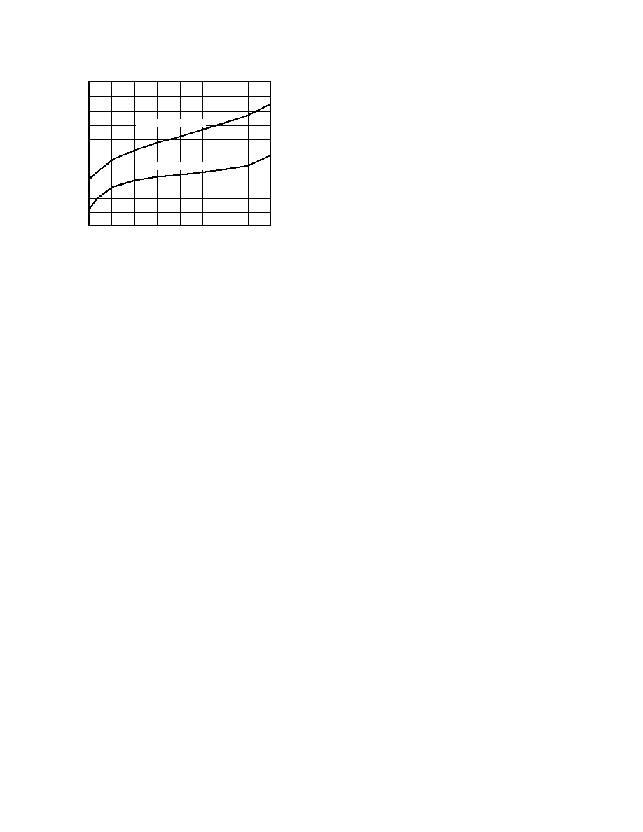
SUPPLY VOLTAGE (AVDD & DVDD) – Volts
0
2.85
0.9
1.0
0.8
0.7
0.6
0.5
0.4
0.3
0.2
0.1
3.15
3.45
4.05
4.35
4.65
4.95
5.25
3.75
MCLK IN = 2.4576MHz
MCLK IN = 1MHz
SUPPLY
CURRENT
(AV
DD
&
DV
DD
)–
mA
Figure 5. IDD vs. Supply Voltage
Grounding and Layout
Since the analog inputs and reference input are differential,
most of the voltages in the analog modulator are common-mode
voltages. The excellent Common-Mode Rejection of the part
will remove common-mode noise on these inputs. The analog
and digital supplies to the AD7714 are independent and sepa-
rately pinned out to minimize coupling between the analog and
digital sections of the device. The digital filter will provide
rejection of broadband noise on the power supplies, except at
integer multiples of the modulator sampling frequency. The
digital filter also removes noise from the analog and reference
inputs provided those noise sources do not saturate the analog
modulator. As a result, the AD7714 is more immune to noise
interference that a conventional high resolution converter. How-
ever, because the resolution of the AD7714 is so high and the
noise levels from the AD7714 so low, care must be taken with
regard to grounding and layout.
The printed circuit board which houses the AD7714 should be
designed such that the analog and digital sections are separated
and confined to certain areas of the board. This facilitates the
use of ground planes which can be separated easily. A minimum
etch technique is generally best for ground planes as it gives the
best shielding. Digital and analog ground planes should only be
joined in one place. If the AD7714 is the only device requiring
an AGND to DGND connection, then the ground planes
should be connected at the AGND and DGND pins of the
AD7714. If the AD7714 is in a system where multiple devices
require AGND to DGND connections, the connection should
still be made at one point only, a star ground point which
should be established as close as possible to the AD7714.
Avoid running digital lines under the device as these will couple
noise onto the die. The analog ground plane should be allowed
to run under the AD7714 to avoid noise coupling. The power
supply lines to the AD7714 should use as large a trace as pos-
sible to provide low impedance paths and reduce the effects of
glitches on the power supply line. Fast switching signals like
clocks should be shielded with digital ground to avoid radiating
noise to other sections of the board and clock signals should
never be run near the analog inputs. Avoid crossover of digital
and analog signals. Traces on opposite sides of the board should
run at right angles to each other. This will reduce the effects of
feedthrough through the board. A microstrip technique is by far
the best but is not always possible with a double-sided board. In
this technique, the component side of the board is dedicated to
ground planes while signals are placed on the solder side.
Good decoupling is important when using high resolution
ADCs. All analog supplies should be decoupled with 10
F
tantalum in parallel with 0.1
F capacitors to AGND. To
achieve the best from these decoupling components, they have
to be placed as close as possible to the device, ideally right up
against the device. All logic chips should be decoupled with
0.1
F disc ceramic capacitors to DGND. In systems where a
common supply voltage is used to drive both the AVDD and
DVDD of the AD7714, it is recommended that the system’s
AVDD supply is used. This supply should have the recommended
analog supply decoupling capacitors between the AVDD pin of
the AD7714 and AGND and the recommended digital supply
decoupling capacitor between the DVDD pin of the AD7714 and
DGND.
Evaluating the AD7714 Performance
The recommended layout for the AD7714 is outlined in the
evaluation board for the AD7714. The evaluation board pack-
age includes a fully assembled and tested evaluation board,
documentation, software for controlling the board over the
printer port of a PC and software for analyzing the AD7714’s
performance on the PC. For the AD7714-5, the evaluation
board order number is EVAL-AD7714-5EB and for the AD7714-3,
the order number is EVAL-AD7714-3EB.
Noise levels in the signals applied to the AD7714 may also
affect performance of the part. The AD7714 allows two tech-
niques for evaluating the true performance of the part, indepen-
dent of the analog input signal. These schemes should be used
after a calibration has been performed on the part.
The first of these is to select the AIN6/AIN6 input channel
arrangement. In this case, the differential inputs to the AD7714
are internally shorted together to provide a zero differential
voltage for the analog modulator. External to the device, the
AIN6 input should be connected to a voltage that is within the
allowable common-mode range of the part.
The second scheme is to evaluate the part with a voltage near
the input full scale voltage for a gain of 1. To do this, the refer-
ence voltage for the part should be applied to the analog input.
This will give a fixed full-scale reading from the device. If the
zero-scale calibration coefficient is now read from the device,
increased by a number equivalent to about 200 decimal and this
value reloaded to the zero-scale calibration register, the input
range will be offset such that a voltage equal to reference voltage
no longer corresponds to a full-scale reading. This allows the
user to evaluate the noise performance of the part with a near
full-scale voltage.
相关PDF资料 |
PDF描述 |
|---|---|
| VI-2WW-MY | CONVERTER MOD DC/DC 5.5V 50W |
| SP208EET-L/TR | IC TXRX RS232 ESD LP 24SOIC |
| AD9218BSTZ-RL65 | IC ADC 10BIT DUAL 65MSPS 48-LQFP |
| SP208EEA-L/TR | IC TXRX RS232 ESD LP 24SSOP |
| VI-2W0-MY | CONVERTER MOD DC/DC 5V 50W |
相关代理商/技术参数 |
参数描述 |
|---|---|
| AD7714YRZ | 制造商:Analog Devices 功能描述:IC ADC 24-BIT SIGMA DELTA |
| AD7714YRZ-REEL | 功能描述:IC ADC 24BIT SIGMA-DELTA 24SOIC RoHS:是 类别:集成电路 (IC) >> 数据采集 - 模数转换器 系列:- 标准包装:1,000 系列:- 位数:12 采样率(每秒):300k 数据接口:并联 转换器数目:1 功率耗散(最大):75mW 电压电源:单电源 工作温度:0°C ~ 70°C 安装类型:表面贴装 封装/外壳:24-SOIC(0.295",7.50mm 宽) 供应商设备封装:24-SOIC 包装:带卷 (TR) 输入数目和类型:1 个单端,单极;1 个单端,双极 |
| AD7714YRZ-REEL7 | 功能描述:IC ADC 24BIT SIGMA-DELTA 24SOIC RoHS:是 类别:集成电路 (IC) >> 数据采集 - 模数转换器 系列:- 标准包装:1,000 系列:- 位数:12 采样率(每秒):300k 数据接口:并联 转换器数目:1 功率耗散(最大):75mW 电压电源:单电源 工作温度:0°C ~ 70°C 安装类型:表面贴装 封装/外壳:24-SOIC(0.295",7.50mm 宽) 供应商设备封装:24-SOIC 包装:带卷 (TR) 输入数目和类型:1 个单端,单极;1 个单端,双极 |
| AD7715 | 制造商:AD 制造商全称:Analog Devices 功能描述:3 V/5 V, 450 uA 16-Bit, Sigma-Delta ADC |
发布紧急采购,3分钟左右您将得到回复。