- 您现在的位置:买卖IC网 > PDF目录10204 > AD7714YRZ (Analog Devices Inc)IC ADC 24BIT SIGMA-DELTA 24SOIC PDF资料下载
参数资料
| 型号: | AD7714YRZ |
| 厂商: | Analog Devices Inc |
| 文件页数: | 38/40页 |
| 文件大小: | 0K |
| 描述: | IC ADC 24BIT SIGMA-DELTA 24SOIC |
| 标准包装: | 31 |
| 位数: | 24 |
| 采样率(每秒): | 1k |
| 数据接口: | DSP,MICROWIRE?,QSPI?,串行,SPI? |
| 转换器数目: | 1 |
| 功率耗散(最大): | 7mW |
| 电压电源: | 模拟和数字 |
| 工作温度: | -40°C ~ 105°C |
| 安装类型: | 表面贴装 |
| 封装/外壳: | 24-SOIC(0.295",7.50mm 宽) |
| 供应商设备封装: | 24-SOIC W |
| 包装: | 管件 |
| 输入数目和类型: | 3 个差分,单极;3 个差分,双极;5 个伪差分,单极;5 个伪差分,双极 |
| 配用: | EVAL-AD7714-3EBZ-ND - BOARD EVAL FOR AD7714 |
第1页第2页第3页第4页第5页第6页第7页第8页第9页第10页第11页第12页第13页第14页第15页第16页第17页第18页第19页第20页第21页第22页第23页第24页第25页第26页第27页第28页第29页第30页第31页第32页第33页第34页第35页第36页第37页当前第38页第39页第40页
2
AD7714
REV. C
–7–
ORDERING GUIDE
AVDD
Temperature
Package
Model
Supply
Range
Option*
AD7714AN-5
5 V
–40
°C to +85°C
N-24
AD7714AR-5
5 V
–40
°C to +85°C
R-24
AD7714ARS-5
5 V
–40
°C to +85°C
RS-28
AD7714AN-3
3 V
–40
°C to +85°C
N-24
AD7714AR-3
3 V
–40
°C to +85°C
R-24
AD7714ARS-3
3 V
–40
°C to +85°C
RS-28
AD7714YN
3 V/5 V
–40
°C to +105°C
N-24
AD7714YR
3 V/5 V
–40
°C to +105°C
R-24
AD7714YRU
3 V/5 V
–40
°C to +105°C
RU-24
AD7714AChips-5
5 V
–40
°C to +85°CDie
AD7714AChips-3
3 V
–40
°C to +85°CDie
EVAL-AD7714-5EB 5 V
Evaluation Board
EVAL-AD7714-3EB 3 V
Evaluation Board
*N = Plastic DIP; R = SOIC; RS = SSOP; RU = Thin Shrink Small Outline.
TIMING CHARACTERISTICS1, 2
(AVDD = DVDD = +2.7 V to +5.25 V; AGND = DGND = 0 V; fCLKIN = 2.5 MHz; Input Logic 0 = 0 V,
Logic 1 = DVDD unless otherwise noted.)
Limit at TMIN, TMAX
Parameter
(A, Y Versions)
Units
Conditions/Comments
fCLKIN
3, 4
400
kHz min
Master Clock Frequency: Crystal/Resonator or Externally
Supplied
2.5
MHz max
For Specified Performance
tCLK IN LO
0.4
× t
CLK IN
ns min
Master Clock Input Low Time. tCLK IN = 1/fCLK IN
tCLK IN HI
0.4
× t
CLK IN
ns min
Master Clock Input High Time
tDRDY
500
× t
CLK IN
ns nom
DRDY High Time
t1
100
ns min
SYNC Pulsewidth
t2
100
ns min
RESET Pulsewidth
Read Operation
t3
0
ns min
DRDY to CS Setup Time
t4
0
ns min
CS Falling Edge to SCLK Active Edge Setup Time5
t5
6
0
ns min
SCLK Active Edge to Data Valid Delay5
80
ns max
DVDD = +5 V
100
ns max
DVDD = +3 V
t6
100
ns min
SCLK High Pulsewidth
t7
100
ns min
SCLK Low Pulsewidth
t8
0
ns min
CS Rising Edge to SCLK Active Edge Hold Time5
t9
7
10
ns min
Bus Relinquish Time after SCLK Active Edge5
60
ns max
DVDD = +5 V
100
ns max
DVDD = +3 V
t10
100
ns max
SCLK Active Edge to
DRDY High5, 8
Write Operation
t11
0
ns min
CS Falling Edge to SCLK Active Edge Setup Time5
t12
30
ns min
Data Valid to SCLK Edge Setup Time
t13
20
ns min
Data Valid to SCLK Edge Hold Time
t14
100
ns min
SCLK High Pulsewidth
t15
100
ns min
SCLK Low Pulsewidth
t16
0
ns min
CS Rising Edge to SCLK Edge Hold Time
NOTES
1Sample tested at +25
°C to ensure compliance. All input signals are specified with tr = tf = 5 ns (10% to 90% of DV
DD) and timed from a voltage level of 1.6 V.
2See Figures 6 and 7. Timing applies for all grades.
3CLKIN Duty Cycle range is 45% to 55%. CLKIN must be supplied whenever the AD7714 is not in standby mode. If no clock is present in this case, the device can
draw higher current than specified and possibly become uncalibrated.
4The AD7714 is production tested with f
CLKIN at 2.4576 MHz (1 MHz for some IDD tests). It is guaranteed by characterization to operate at 400 kHz.
5SCLK active edge is falling edge of SCLK with POL = 1; SCLK active edge is rising edge of SCLK with POL = 0.
6These numbers are measured with the load circuit of Figure 1 and defined as the time required for the output to cross the V
OL or VOH limits.
7These numbers are derived from the measured time taken by the data output to change 0.5 V when loaded with the circuit of Figure 1. The measured number is then
extrapolated back to remove effects of charging or discharging the 100 pF capacitor. This means that the times quoted in the timing characteristics are the true bus
relinquish times of the part and as such are independent of external bus loading capacitances.
8
DRDY returns high after the first read from the device after an output update. The same data can be read again, if required, while DRDY is high although care
should be taken that subsequent reads do not occur close to the next output update.
Specifications subject to change without notice.
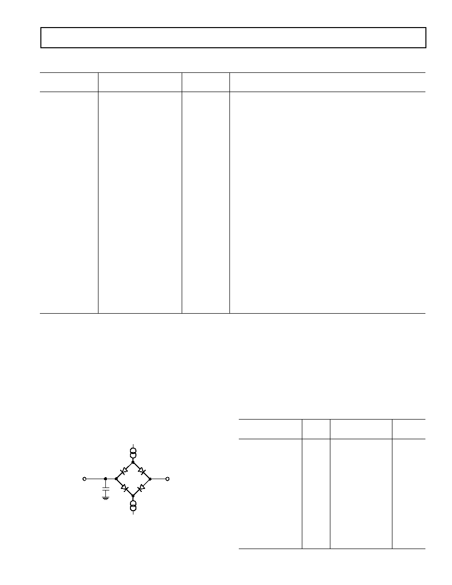
Figure 1. Load Circuit for Access Time and Bus
Relinquish Time
TO OUTPUT
PIN
50pF
ISINK (800 A AT DVDD = +5V
100 A AT DVDD = +3.3V)
+1.6V
ISOURCE (200 A AT DVDD = +5V
100 A AT DVDD = +3.3V)
相关PDF资料 |
PDF描述 |
|---|---|
| VI-2WW-MY | CONVERTER MOD DC/DC 5.5V 50W |
| SP208EET-L/TR | IC TXRX RS232 ESD LP 24SOIC |
| AD9218BSTZ-RL65 | IC ADC 10BIT DUAL 65MSPS 48-LQFP |
| SP208EEA-L/TR | IC TXRX RS232 ESD LP 24SSOP |
| VI-2W0-MY | CONVERTER MOD DC/DC 5V 50W |
相关代理商/技术参数 |
参数描述 |
|---|---|
| AD7714YRZ | 制造商:Analog Devices 功能描述:IC ADC 24-BIT SIGMA DELTA |
| AD7714YRZ-REEL | 功能描述:IC ADC 24BIT SIGMA-DELTA 24SOIC RoHS:是 类别:集成电路 (IC) >> 数据采集 - 模数转换器 系列:- 标准包装:1,000 系列:- 位数:12 采样率(每秒):300k 数据接口:并联 转换器数目:1 功率耗散(最大):75mW 电压电源:单电源 工作温度:0°C ~ 70°C 安装类型:表面贴装 封装/外壳:24-SOIC(0.295",7.50mm 宽) 供应商设备封装:24-SOIC 包装:带卷 (TR) 输入数目和类型:1 个单端,单极;1 个单端,双极 |
| AD7714YRZ-REEL7 | 功能描述:IC ADC 24BIT SIGMA-DELTA 24SOIC RoHS:是 类别:集成电路 (IC) >> 数据采集 - 模数转换器 系列:- 标准包装:1,000 系列:- 位数:12 采样率(每秒):300k 数据接口:并联 转换器数目:1 功率耗散(最大):75mW 电压电源:单电源 工作温度:0°C ~ 70°C 安装类型:表面贴装 封装/外壳:24-SOIC(0.295",7.50mm 宽) 供应商设备封装:24-SOIC 包装:带卷 (TR) 输入数目和类型:1 个单端,单极;1 个单端,双极 |
| AD7715 | 制造商:AD 制造商全称:Analog Devices 功能描述:3 V/5 V, 450 uA 16-Bit, Sigma-Delta ADC |
发布紧急采购,3分钟左右您将得到回复。