- 您现在的位置:买卖IC网 > PDF目录378276 > AD7739 (Analog Devices, Inc.) 8-Channel, High Throughput, 24-Bit Sigma-Delta ADC PDF资料下载
参数资料
| 型号: | AD7739 |
| 厂商: | Analog Devices, Inc. |
| 元件分类: | ADC |
| 英文描述: | 8-Channel, High Throughput, 24-Bit Sigma-Delta ADC |
| 中文描述: | 8通道,高吞吐量,24位Σ-Δ模数转换器 |
| 文件页数: | 26/32页 |
| 文件大小: | 380K |
| 代理商: | AD7739 |
第1页第2页第3页第4页第5页第6页第7页第8页第9页第10页第11页第12页第13页第14页第15页第16页第17页第18页第19页第20页第21页第22页第23页第24页第25页当前第26页第27页第28页第29页第30页第31页第32页

AD7739
CIRCUIT DESCRIPTION
The AD7739 is a high precision analog-to-digital converter that
is intended for the measurement of wide dynamic range, low
frequency signals in industrial process control, instrumentation,
and PLC systems.
Rev. 0 | Page 26 of 32
It contains a multiplexer, an input buffer, a sigma-delta
(or charge balancing) ADC, a digital filter, a clock oscillator,
a digital I/O port, and a serial communications interface.
ANALOG INPUTS
The AD7739 has nine analog input pins connected to the ADC
through the internal multiplexer. The analog front end can be
configured as eight single-ended inputs or four differential
inputs or any combination of these (via the channel setup
registers).
The AD7739 contains a wide bandwidth, fast settling time
differential input buffer capable of driving the dynamic load of
a high speed sigma-delta modulator. With the internal buffer
enabled, the analog inputs feature high input impedance.
If chopping is enabled or when switching between channels,
there is a dynamic current on analog inputs charging the
internal capacitance of the multiplexer and input buffer. The
capacitance is approximately 10 pF.
At the start of each conversion, there is a delay to allow the
capacitance to be charged (see the Multiplexer, Conversion, and
Data Output Timing section). If the analog inputs resistive
source impedance does not exceed 50 k, the internal
capacitance is charged fast enough and the AD7739
performance is not affected at the 16-bit level.
An external RC filter connected to the analog inputs would
average the multiplexer channel-to-channel switching dynamic
currents to a dc current leading to a dc voltage drop across the
external input resistance. To avoid additional gain errors, offset
errors, and channel-to-channel crosstalk due to this effect, low
resistor values should be used in the low-pass RC filter for the
AD7739. The recommended low-pass RC filter for the analog
inputs is 100 and 100 nF.
The average (dc) current, charging the capacitance on the
multiplexer output, is related to the equation:
I
≈
C
MUX
× V
MUX
× F
S
Where
C
MUX
is the capacitance on the multiplexer output,
approximately 10 pF ,
V
MUX
is the voltage difference on the
multiplexer output between two subsequent conversions, which
can be up to 5 V, and
F
S
is the channel sampling frequency,
which relates to the sum of conversion times on all
subsequently sampled channels.
SIGMA-DELTA ADC
The AD7739 core consists of a charge balancing sigma-delta
modulator and a digital filter. The architecture is optimized for
fast, fully settled conversion. This allows for fast channel-to-
channel switching while maintaining inherently excellent
linearity, high resolution, and low noise.
CHOPPING
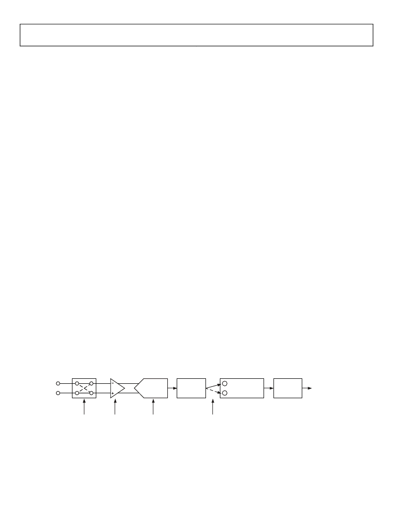
With chopping enabled, the multiplexer repeatedly reverses the
ADC inputs. Every output data result is then calculated as an
average of two conversions, the first with the positive and the
second with the negative offset term included. This effectively
removes any offset error of the input buffer and sigma-delta
modulator. Figure 23 shows the channel signal chain with
chopping enabled.
MULTIPLEXER
+
DIGITAL
FILTER
Σ
-
MODULATOR
BUFFER
–
SCALING
ARITHMETIC
(CALIBRATIONS)
CHOP
CHOP
CHOP
f
MCLK
/2
DIGITAL
INTERFACE
OUTPUT DATA
AT THE SELECTED
DATA RATE
AIN(+)
AIN(–)
03742-0-023
Figure 23. Channel Signal Chain Diagram with Chopping Enabled
相关PDF资料 |
PDF描述 |
|---|---|
| AD7739BRU | 8-Channel, High Throughput, 24-Bit Sigma-Delta ADC |
| AD7739BRU-REEL | 8-Channel, High Throughput, 24-Bit Sigma-Delta ADC |
| AD7739BRU-REEL7 | 8-Channel, High Throughput, 24-Bit Sigma-Delta ADC |
| AD79024 | LC2MOS 20-Bit Data Acquisition System |
| AD8152 | 34 x 34, 3.2 Gbps Asynchronous Digital Crosspoint Switch |
相关代理商/技术参数 |
参数描述 |
|---|---|
| AD7739BRU | 功能描述:IC ADC 24BIT 8-CH 24-TSSOP RoHS:否 类别:集成电路 (IC) >> 数据采集 - 模数转换器 系列:- 标准包装:1,000 系列:- 位数:12 采样率(每秒):300k 数据接口:并联 转换器数目:1 功率耗散(最大):75mW 电压电源:单电源 工作温度:0°C ~ 70°C 安装类型:表面贴装 封装/外壳:24-SOIC(0.295",7.50mm 宽) 供应商设备封装:24-SOIC 包装:带卷 (TR) 输入数目和类型:1 个单端,单极;1 个单端,双极 |
| AD7739BRU-REEL | 功能描述:IC ADC 24BIT 8CH SIG-DEL 24TSSOP RoHS:否 类别:集成电路 (IC) >> 数据采集 - 模数转换器 系列:- 标准包装:1,000 系列:- 位数:12 采样率(每秒):300k 数据接口:并联 转换器数目:1 功率耗散(最大):75mW 电压电源:单电源 工作温度:0°C ~ 70°C 安装类型:表面贴装 封装/外壳:24-SOIC(0.295",7.50mm 宽) 供应商设备封装:24-SOIC 包装:带卷 (TR) 输入数目和类型:1 个单端,单极;1 个单端,双极 |
| AD7739BRU-REEL7 | 制造商:Analog Devices 功能描述:ADC Single Delta-Sigma 3.05Msps 24-bit Serial 24-Pin TSSOP T/R 制造商:Analog Devices 功能描述:ADC SGL DELTA-SIGMA 15.133KSPS 24BIT SERL 24TSSOP - Tape and Reel |
| AD7739BRUZ | 功能描述:IC ADC 24BIT 8-CH 24-TSSOP RoHS:是 类别:集成电路 (IC) >> 数据采集 - 模数转换器 系列:- 标准包装:1 系列:microPOWER™ 位数:8 采样率(每秒):1M 数据接口:串行,SPI? 转换器数目:1 功率耗散(最大):- 电压电源:模拟和数字 工作温度:-40°C ~ 125°C 安装类型:表面贴装 封装/外壳:24-VFQFN 裸露焊盘 供应商设备封装:24-VQFN 裸露焊盘(4x4) 包装:Digi-Reel® 输入数目和类型:8 个单端,单极 产品目录页面:892 (CN2011-ZH PDF) 其它名称:296-25851-6 |
| AD7739BRUZ | 制造商:Analog Devices 功能描述:IC, ADC, 24BIT, 15.1KSPS, TSSOP-24 |
发布紧急采购,3分钟左右您将得到回复。