- 您现在的位置:买卖IC网 > PDF目录378276 > AD7739BRU-REEL (ANALOG DEVICES INC) 8-Channel, High Throughput, 24-Bit Sigma-Delta ADC PDF资料下载
参数资料
| 型号: | AD7739BRU-REEL |
| 厂商: | ANALOG DEVICES INC |
| 元件分类: | ADC |
| 英文描述: | 8-Channel, High Throughput, 24-Bit Sigma-Delta ADC |
| 中文描述: | 8-CH 24-BIT DELTA-SIGMA ADC, SERIAL ACCESS, PDSO24 |
| 封装: | MS-153AD, TSSOP-24 |
| 文件页数: | 23/32页 |
| 文件大小: | 380K |
| 代理商: | AD7739BRU-REEL |
第1页第2页第3页第4页第5页第6页第7页第8页第9页第10页第11页第12页第13页第14页第15页第16页第17页第18页第19页第20页第21页第22页当前第23页第24页第25页第26页第27页第28页第29页第30页第31页第32页
AD7739
RESET
The AD7739 can be reset by the RESET pin or by writing a reset
sequence to the AD7739 serial interface. The reset sequence is
N × 0 + 32 × 1, which could be the data sequence 0x00 + 0xFF +
0xFF + 0xFF + 0xFF in a byte-oriented interface.
Rev. 0 | Page 23 of 32
The AD7739 also features a power-on reset with a trip point
of 2 V and goes to the defined default state after power-on.
It is the system designer’s responsibility to prevent an unwanted
write operation to the AD7739. The unwanted write operation
could happen when a spurious clock appears on the SCLK while
the CS pin is low. Note that if the AD7739 interface signals are
floating or undefined at system power-on, the part can be
inadvertently configured into an unknown state. This could be
easily overcome by initiating either a hardware reset event or a
32 ones reset sequence as the first step in the system
configuration.
ACCESS THE AD7739 REGISTERS
All communications to the part start with a write operation to
the communications register followed by either reading or
writing the addressed register. In a simultaneous read-write
interface (such as SPI), write 0 to the AD7739 while reading
data.
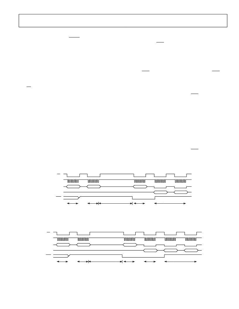
Figure 16 shows the AD7739 interface read sequence for the
ADC status register.
SINGLE CONVERSION AND READING DATA
When the mode register is being written, the ADC status byte
is cleared and the RDY pin goes high, regardless of its previous
state. When the single conversion command is written to the
mode register, the ADC starts the conversion on the channel
selected by the address of the mode register. After the
conversion is completed, the data register is updated, the mode
register is changed to idle mode, the relevant RDY bit is set,
and the RDY pin goes low. The RDY bit is reset and the RDY
pin returns high when the relevant channel data register is
being read.
Figure 17 shows the digital interface signals executing a single
conversion on Channel 0, waiting for the RDY pin to go low,
and reading the Channel 0 data register.
DUMP MODE
When the DUMP bit in the mode register is set to 1, the channel
status register will be read immediately by a read of the channel
data register, regardless of whether the status or the data register
has been addressed through the communications register. The
DIN pin should not be high while reading 24-bit data in dump
mode; otherwise, the AD7739 will be reset.
Figure 18 shows the digital interface signals executing a single
conversion on Channel 0, waiting for the RDY pin to go low,
and reading the Channel 0 status register and data register in
the dump mode.
DIN
SCLK
CS
DOUT
WRITE
COMMUNICATIONS
REGISTER
WRITE
MODE
REGISTER
RDY
CONVERSION TIME
READ DATA REGISTER
0x38
0x40
0x48
(0x00)
(0x00)
DATA
DATA
WRITE
COMMUNICATIONS
REGISTER
03742-0-017
Figure 17. Serial Interface Signals—Single Conversion Command and 16-Bit Data Reading
DIN
SCLK
CS
DOUT
WRITE
COMMUNICATIONS
REGISTER
WRITE
MODE
REGISTER
RDY
CONVERSION TIME
READ DATA
REGISTER
READ
CHANNEL
STATUS
0x38
0x48
0x48
WRITE
COMMUNICATIONS
REGISTER
(0x00)
(0x00)
(0x00)
STATUS
DATA
DATA
03742-0-018
Figure 18. Serial Interface Signals—Single Conversion Command, 16-Bit Data Reading, Dump Mode
相关PDF资料 |
PDF描述 |
|---|---|
| AD7739BRU-REEL7 | 8-Channel, High Throughput, 24-Bit Sigma-Delta ADC |
| AD79024 | LC2MOS 20-Bit Data Acquisition System |
| AD8152 | 34 x 34, 3.2 Gbps Asynchronous Digital Crosspoint Switch |
| AD8152-EVAL | 34 x 34, 3.2 Gbps Asynchronous Digital Crosspoint Switch |
| AD8152JBP | 34 x 34, 3.2 Gbps Asynchronous Digital Crosspoint Switch |
相关代理商/技术参数 |
参数描述 |
|---|---|
| AD7739BRU-REEL7 | 制造商:Analog Devices 功能描述:ADC Single Delta-Sigma 3.05Msps 24-bit Serial 24-Pin TSSOP T/R 制造商:Analog Devices 功能描述:ADC SGL DELTA-SIGMA 15.133KSPS 24BIT SERL 24TSSOP - Tape and Reel |
| AD7739BRUZ | 功能描述:IC ADC 24BIT 8-CH 24-TSSOP RoHS:是 类别:集成电路 (IC) >> 数据采集 - 模数转换器 系列:- 标准包装:1 系列:microPOWER™ 位数:8 采样率(每秒):1M 数据接口:串行,SPI? 转换器数目:1 功率耗散(最大):- 电压电源:模拟和数字 工作温度:-40°C ~ 125°C 安装类型:表面贴装 封装/外壳:24-VFQFN 裸露焊盘 供应商设备封装:24-VQFN 裸露焊盘(4x4) 包装:Digi-Reel® 输入数目和类型:8 个单端,单极 产品目录页面:892 (CN2011-ZH PDF) 其它名称:296-25851-6 |
| AD7739BRUZ | 制造商:Analog Devices 功能描述:IC, ADC, 24BIT, 15.1KSPS, TSSOP-24 |
| AD7739BRUZ-REEL7 | 功能描述:IC ADC 24BIT 8CH SIG-DEL 24TSSOP RoHS:是 类别:集成电路 (IC) >> 数据采集 - 模数转换器 系列:- 标准包装:1,000 系列:- 位数:12 采样率(每秒):300k 数据接口:并联 转换器数目:1 功率耗散(最大):75mW 电压电源:单电源 工作温度:0°C ~ 70°C 安装类型:表面贴装 封装/外壳:24-SOIC(0.295",7.50mm 宽) 供应商设备封装:24-SOIC 包装:带卷 (TR) 输入数目和类型:1 个单端,单极;1 个单端,双极 |
| AD773A | 制造商:AD 制造商全称:Analog Devices 功能描述:10-Bit, 20 MSPS Monolithic A/D Converter |
发布紧急采购,3分钟左右您将得到回复。