- 您现在的位置:买卖IC网 > PDF目录10664 > AD7764BRUZ (Analog Devices Inc)IC ADC 24BIT S/D 312KSPS 28TSSOP PDF资料下载
参数资料
| 型号: | AD7764BRUZ |
| 厂商: | Analog Devices Inc |
| 文件页数: | 16/33页 |
| 文件大小: | 0K |
| 描述: | IC ADC 24BIT S/D 312KSPS 28TSSOP |
| 标准包装: | 1 |
| 位数: | 24 |
| 采样率(每秒): | 312k |
| 数据接口: | 串行,SPI? |
| 转换器数目: | 1 |
| 功率耗散(最大): | 371mW |
| 电压电源: | 模拟和数字 |
| 工作温度: | -40°C ~ 85°C |
| 安装类型: | 表面贴装 |
| 封装/外壳: | 28-TSSOP(0.173",4.40mm 宽) |
| 供应商设备封装: | 28-TSSOP |
| 包装: | 管件 |
| 输入数目和类型: | 1 个差分,单极;1 个差分,双极 |
| 产品目录页面: | 779 (CN2011-ZH PDF) |
第1页第2页第3页第4页第5页第6页第7页第8页第9页第10页第11页第12页第13页第14页第15页当前第16页第17页第18页第19页第20页第21页第22页第23页第24页第25页第26页第27页第28页第29页第30页第31页第32页第33页
AD7764
Rev. A | Page 22 of 32
AD7764 FUNCTIONALITY
SYNCHRONIZATION
The SYNC input to the AD7764 provides a synchronization
function that allows the user to begin gathering samples of the
analog front-end input from a known point in time.
The SYNC function allows multiple AD7764 devices, operated
from the same master clock that use common SYNC and
RESET signals, to be synchronized so that each ADC
simultaneously updates its output register. Note that all devices
being synchro-nized must operate in the same power mode and
at the same decimation rate.
In the case of a system with multiple AD7764s, connect
common MCLK, SYNC and RESET signals to each AD7764.
The AD7764 SYNC pin is polled by the falling edge of MCLK.
The AD7764 device goes into SYNC when an MCLK falling
edge senses that the SYNC input signal is logic low. At this
point, the digital filter sequencer is reset to 0. The filter is held
in a reset state (in SYNC mode) until the first MCLK falling
edge senses SYNC
Where possible, ensure that all transitions of
to be logic high
SYNC occur
synchronously with the rising edge of MCLK (that is, as far
away as possible from the MCLK falling edge, or decision edge).
Otherwise, abide by the timing specified in Figure 41, which
excludes the SYNC
Keep
rising edge from occurring in a 10 ns
window centered around the MCLK fallings edge.
SYNC logic low for a minimum of four MCLK periods.
When the MCLK falling edge senses that SYNC has returned to
logic high, the AD7764 filters begin to gather input samples
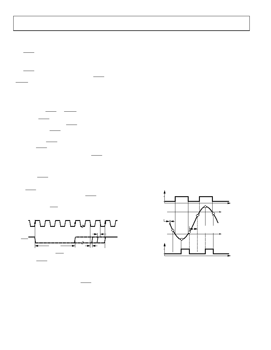
simultaneously. The FSO
06518-
303
MCLK
SYNC
tS MIN
4 ×
tMCLK
tS HOLD
tS SETUP
falling edges are also synchronized,
allowing for simultaneous output of conversion data.
Figure 41. SYNC
Following a
Timing Relative to MCLK
SYNC, the digital filter needs time to settle before
valid data can be read from the AD7764. The user knows there
is valid data on the SDO line by checking the FILTER-SETTLE
status bit (see D7 in Table 9) that is output with each conversion
result. The time from the rising edge of SYNC
OVERRANGE ALERTS
until the FILTER-
SETTLE bit asserts depends on the filter configuration used. See
the Theory of Operation section and the values listed in Table 6
for details on calculating the time until FILTER-SETTLE asserts.
Note that the FILTER_SETTLE bit is designed as a reactionary
flag to indicate when the conversion data output is valid.
The AD7764 offers an overrange function in both a pin and
status bit output. The overrange alerts indicate when the voltage
applied to the AD7764 modulator input pins exceeds the limit
set in the overrange register, indicating that the voltage applied
is approaching a level where the modulator will be overranged.
To set this limit, the user must program the register. The default
overrange limit is set to 80% of the VREF voltage (see the
AD7764 Registers section).
The OVERRANGE pin outputs logic high to alert the user
that the modulator has sampled an input voltage greater in
magnitude than the overrange limit as set in the overrange
register. The OVERRANGE pin is set to logic high when the
modulator samples an input above the overrange limit. After
the input returns below the limit, the OVERRANGE pin returns
to zero. The OVERRANGE pin is updated after the first FIR
filter stage. Its output changes at the ICLK/4 frequency.
The OVR status bit is output as Bit D6 on SDO during a data
conversion and can be checked in the AD7764 status register.
This bit is less dynamic than the OVERRANGE pin output. It is
updated on each conversion result output; that is, the bit changes
at the output data rate. If the modulator has sampled a voltage
input that exceeded the overrange limit during the process of
gathering samples for a particular conversion result output,
then the OVR bit is set to logic high.
O
V
E
RRANG
E
P
IN
O
UT
P
UT
LOGIC
LEVEL
HIGH
LOW
O
V
R
BI
T
LOGIC
LEVEL
HIGH
LOW
OUTPUT FREQUENCY
OF FIR FILTER 1 = ICLK/4
OVERRANGE
LIMIT
OVERRANGE
LIMIT
OBSOLUTE INPUT
TO AD7764
[(VIN+) – (VIN–)]
OUTPUT DATA RATE (ODR)
(ICLK/DECIMATION RATE
t
06518-
016
Figure 42. OVERRANGE Pin and OVR Bit vs. Absolute Voltage
Applied to the Modulator
The output points from FIR Filter 1 in Figure 42 are not drawn
to scale relative to the output data rate points. The FIR Filter 1
output is updated either 16×, 32×, or 64× faster than the output
data rate, depending on the decimation rate in operation.
相关PDF资料 |
PDF描述 |
|---|---|
| AD7357BRUZ | IC ADC DUAL14BIT 4.2MSPS 16TSSOP |
| AD7731BRZ | IC ADC 24BIT SIGMA-DELTA 24-SOIC |
| LTC2355IMSE-14#PBF | IC ADC 14BIT 3.5MSPS 10-MSOP |
| MAX9092AUA+T | IC COMPARATOR GP DUAL 8UMAX |
| VI-B13-MX-F4 | CONVERTER MOD DC/DC 24V 75W |
相关代理商/技术参数 |
参数描述 |
|---|---|
| AD7764BRUZ-REEL7 | 功能描述:IC ADC 24BIT S/D 312KSPS 28TSSOP RoHS:是 类别:集成电路 (IC) >> 数据采集 - 模数转换器 系列:- 标准包装:1,000 系列:- 位数:12 采样率(每秒):300k 数据接口:并联 转换器数目:1 功率耗散(最大):75mW 电压电源:单电源 工作温度:0°C ~ 70°C 安装类型:表面贴装 封装/外壳:24-SOIC(0.295",7.50mm 宽) 供应商设备封装:24-SOIC 包装:带卷 (TR) 输入数目和类型:1 个单端,单极;1 个单端,双极 |
| AD7765 | 制造商:AD 制造商全称:Analog Devices 功能描述:24-Bit, 8.5 mW, 109 dB, 128/64/32 kSPS ADCs |
| AD7765_07 | 制造商:AD 制造商全称:Analog Devices 功能描述:24-Bit, 156 kSPS, 112 dB ヒ-ツ ADC with On-Chip Buffers and Serial Interface |
| AD7765BRUZ | 功能描述:IC ADC 24BIT S/D 156KSPS 28TSSOP RoHS:是 类别:集成电路 (IC) >> 数据采集 - 模数转换器 系列:- 其它有关文件:TSA1204 View All Specifications 标准包装:1 系列:- 位数:12 采样率(每秒):20M 数据接口:并联 转换器数目:2 功率耗散(最大):155mW 电压电源:模拟和数字 工作温度:-40°C ~ 85°C 安装类型:表面贴装 封装/外壳:48-TQFP 供应商设备封装:48-TQFP(7x7) 包装:Digi-Reel® 输入数目和类型:4 个单端,单极;2 个差分,单极 产品目录页面:1156 (CN2011-ZH PDF) 其它名称:497-5435-6 |
| AD7765BRUZ-REEL7 | 功能描述:IC ADC 24BIT S/D 156KSPS 28TSSOP RoHS:是 类别:集成电路 (IC) >> 数据采集 - 模数转换器 系列:- 标准包装:1,000 系列:- 位数:12 采样率(每秒):300k 数据接口:并联 转换器数目:1 功率耗散(最大):75mW 电压电源:单电源 工作温度:0°C ~ 70°C 安装类型:表面贴装 封装/外壳:24-SOIC(0.295",7.50mm 宽) 供应商设备封装:24-SOIC 包装:带卷 (TR) 输入数目和类型:1 个单端,单极;1 个单端,双极 |
发布紧急采购,3分钟左右您将得到回复。