- 您现在的位置:买卖IC网 > PDF目录10667 > AD7767BRUZ-1 (Analog Devices Inc)ADC 24BIT 64KSPS SAR 16-TSSOP PDF资料下载
参数资料
| 型号: | AD7767BRUZ-1 |
| 厂商: | Analog Devices Inc |
| 文件页数: | 8/25页 |
| 文件大小: | 0K |
| 描述: | ADC 24BIT 64KSPS SAR 16-TSSOP |
| 标准包装: | 1 |
| 位数: | 24 |
| 采样率(每秒): | 64k |
| 数据接口: | 串行 |
| 转换器数目: | 1 |
| 功率耗散(最大): | 18mW |
| 电压电源: | 模拟和数字 |
| 工作温度: | -40°C ~ 105°C |
| 安装类型: | 表面贴装 |
| 封装/外壳: | 16-TSSOP(0.173",4.40mm 宽) |
| 供应商设备封装: | 16-TSSOP |
| 包装: | 管件 |
| 输入数目和类型: | 1 个差分,单极 |
| 产品目录页面: | 779 (CN2011-ZH PDF) |
| 配用: | EVAL-AD7767EDZ-ND - BOARD EVAL AD7767 128KSPS 108DB EVAL-AD7767-1EDZ-ND - BOARD EVAL AD7767-1 64KSPS 111DB |
AD7767
Rev. C | Page 15 of
24
THEORY OF OPERATION
The AD7767/AD7767-1/AD7767-2 operate using a fully
differential analog input applied to a successive approximation
(SAR) core. The output of the oversampled SAR is filtered using
a linear-phase digital FIR filter. The fully filtered data is output
in a serial format, with the MSB being clocked out first.
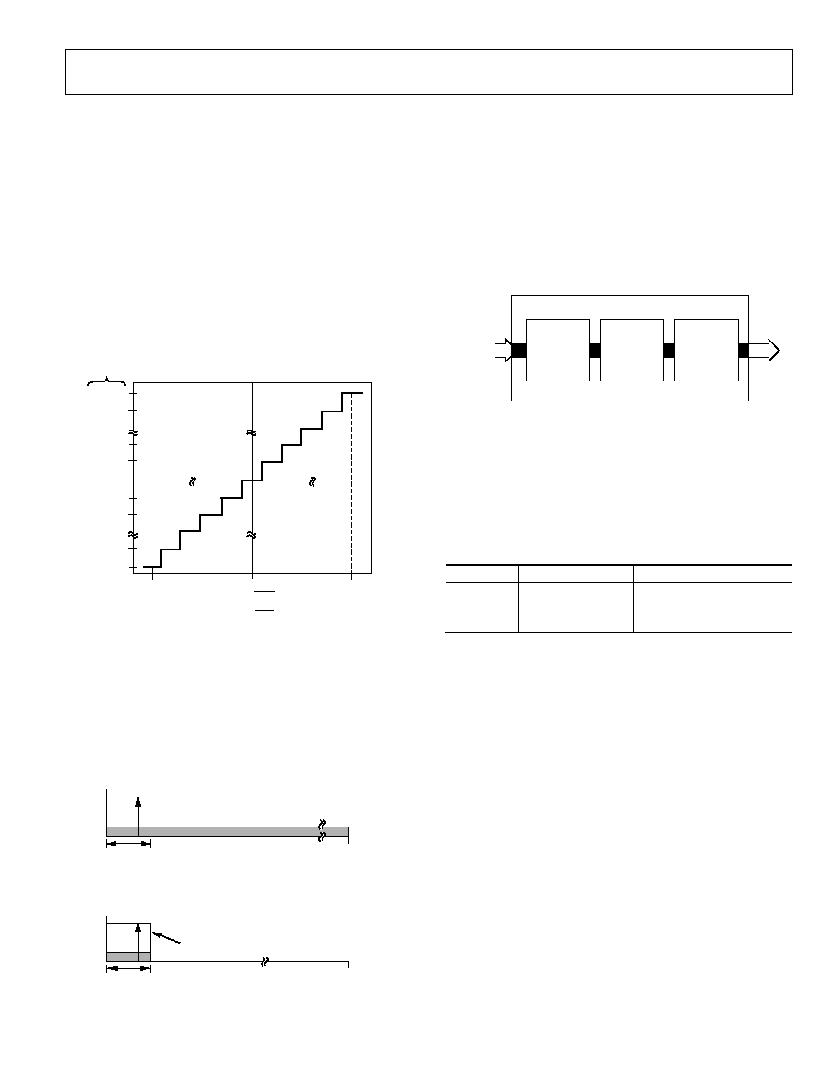
AD7767/AD7767-1/AD7767-2 TRANSFER
FUNCTION
The conversion results of the AD7767/AD7767-1/AD7767-2
are output in a twos complement, 24-bit serial format. The fully
differential inputs VIN+ and VIN are scaled by the AD7767/
AD7767-1/AD7767-2 relative to the reference voltage input
06
85
9-
01
2
100 ... 000
100 ... 001
111 ... 110
111 ... 111
000 ... 000
000 ... 001
000 ... 010
011 ... 110
011 ... 111
24
-B
IT
O
U
T
P
U
T
24 BITS
TWOS
COMPLEMENT
VIN+ = 0V
VIN+ = VREF – 1LSB
VIN– = VREF – 1LSB
VIN– = 0V
VIN+ =
VREF
2
VIN– =
VREF
2
Figure 28. AD7767/AD7767-1/AD7767-2 Transfer Function
CONVERTER OPERATION
Internally, the input waveform applied to the SAR core is
converted and an equivalent digital word is output to the digital
filter at a rate equal to MCLK. By employing oversampling, the
quantization noise of the converter is spread across a wide
bandwidth from 0 to fMCLK. This means that the noise energy
contained in the signal band of interest is reduced (see
QUANTIZATION NOISE
BAND OF INTEREST
fMCLK/2
06
85
9-
2
13
Figure 29. Quantization Noise
DIGITAL FILTER CUTOFF FREQUENCY
fMCLK/2
BAND OF INTEREST
0
68
59
-2
14
Figure 30. Digital Filter Cutoff Frequency
The digital filtering that follows the converter output acts to
remove the out-of-band quantization noise (see Figure 30). This
also has the effect of reducing the data rate from fMCLK at the
input of the filter to fMCLK/8, fMCLK/16, or fMCLK/32 at the digital
output, depending on which model of the device is being used.
The digital filter consists of three separate filter blocks. Figure 31
shows the three constituent blocks of the filter. The order of
decimation of the first filter block is set as 2, 4, or 8. The
remaining sections each operate with a decimation of 2.
06
85
9-
0
1
9
STAGE 1
STAGE 2
DIGITAL FILTER
STAGE 3
SINC FILTER
FIR FILTER
DEC × (2 × n)
DEC × 2
DATA
STREAM
SDO
Figure 31. FIR Filter Stages
(n = 1 for AD7767, n = 2 for AD7767-1, n = 4 for AD7767-2)
Table 6 shows the three available models of the AD7767, listing
the change in output data rate relative to the order of decimation
rate implemented. This brings into focus the trade-off that exists
between extra filtering and reduction in bandwidth, whereby
using a filter option with a larger decimation rate increases the
noise performance while decreasing the usable input bandwidth.
Table 6. AD7767 Models
Model
Decimation Rate
Output Data Rate (ODR)
AD7767
8
128 kHz
AD7767-1
16
64 kHz
AD7767-2
32
32 kHz
Note that the output data rates shown in Table 6 are realized
when using the maximum MCLK input frequency of 1.024 MHz.
The output data rate scales linearly with the MCLK frequency,
as does the digital power dissipated in the device.
The settling time of the filter implemented on the AD7767,
AD7767-1, and AD7767-2 is related to the length of the filter
employed. The response of the filter in the time domain sets the
filter settling time. Table 7 shows the filter settling times of the
AD7767/AD7767-1/AD7767-2.
The frequency responses of the digital filters on the AD7767,
and Figure 34, respectively. At the Nyquist frequency (output
data rate/2), the digital filter provides 6 dB of attenuation. In each
case, the filter provides stop-band attenuation of 100 dB and
pass-band ripple of ±0.005 dB.
相关PDF资料 |
PDF描述 |
|---|---|
| AD7714YRUZ | IC ADC SIGNAL COND 3/5V 24-TSSOP |
| LTC2446IUHF#PBF | IC ADC 24BIT 8CH HI SPEED 38QFN |
| LTC2448IUHF#PBF | IC ADC 24BIT HI SPEED 38QFN |
| LTC2447IUHF#PBF | IC ADC 24BIT 8CH HI SPEED 38QFN |
| LTC2355CMSE-14#PBF | IC ADC 14BIT 3.5MSPS 10-MSOP |
相关代理商/技术参数 |
参数描述 |
|---|---|
| AD7767BRUZ-1-RL7 | 功能描述:ADC 24BIT 10.5MW 64KSPS 16TSSOP RoHS:是 类别:集成电路 (IC) >> 数据采集 - 模数转换器 系列:- 标准包装:1,000 系列:- 位数:12 采样率(每秒):300k 数据接口:并联 转换器数目:1 功率耗散(最大):75mW 电压电源:单电源 工作温度:0°C ~ 70°C 安装类型:表面贴装 封装/外壳:24-SOIC(0.295",7.50mm 宽) 供应商设备封装:24-SOIC 包装:带卷 (TR) 输入数目和类型:1 个单端,单极;1 个单端,双极 |
| AD7767BRUZ-2 | 功能描述:ADC 24BIT 32KSPS SAR 16-TSSOP RoHS:是 类别:集成电路 (IC) >> 数据采集 - 模数转换器 系列:- 其它有关文件:TSA1204 View All Specifications 标准包装:1 系列:- 位数:12 采样率(每秒):20M 数据接口:并联 转换器数目:2 功率耗散(最大):155mW 电压电源:模拟和数字 工作温度:-40°C ~ 85°C 安装类型:表面贴装 封装/外壳:48-TQFP 供应商设备封装:48-TQFP(7x7) 包装:Digi-Reel® 输入数目和类型:4 个单端,单极;2 个差分,单极 产品目录页面:1156 (CN2011-ZH PDF) 其它名称:497-5435-6 |
| AD7767BRUZ-2-RL7 | 功能描述:ADC 24BIT 8.5MW 32KSPS 16TSSOP RoHS:是 类别:集成电路 (IC) >> 数据采集 - 模数转换器 系列:- 标准包装:1,000 系列:- 位数:12 采样率(每秒):300k 数据接口:并联 转换器数目:1 功率耗散(最大):75mW 电压电源:单电源 工作温度:0°C ~ 70°C 安装类型:表面贴装 封装/外壳:24-SOIC(0.295",7.50mm 宽) 供应商设备封装:24-SOIC 包装:带卷 (TR) 输入数目和类型:1 个单端,单极;1 个单端,双极 |
| AD7767BRUZ-RL7 | 功能描述:ADC 24BIT 15MW 128KSPS 16TSSOP RoHS:是 类别:集成电路 (IC) >> 数据采集 - 模数转换器 系列:- 标准包装:1,000 系列:- 位数:12 采样率(每秒):300k 数据接口:并联 转换器数目:1 功率耗散(最大):75mW 电压电源:单电源 工作温度:0°C ~ 70°C 安装类型:表面贴装 封装/外壳:24-SOIC(0.295",7.50mm 宽) 供应商设备封装:24-SOIC 包装:带卷 (TR) 输入数目和类型:1 个单端,单极;1 个单端,双极 |
| AD7768-4BSTZ | 功能描述:24 Bit Analog to Digital Converter 4 Input 4 Sigma-Delta 64-LQFP (10x10) 制造商:analog devices inc. 系列:- 包装:托盘 零件状态:有效 位数:24 采样率(每秒):256k 输入数:4 输入类型:差分 数据接口:SPI 配置:ADC 无线电 - S/H:ADC:- A/D 转换器数:4 架构:三角积分 参考类型:外部 电压 - 电源,模拟:2 V ~ 5.5 V 电压 - 电源,数字:- 特性:同步采样 工作温度:-40°C ~ 150°C 封装/外壳:64-LQFP 供应商器件封装:64-LQFP(10x10) 标准包装:1 |
发布紧急采购,3分钟左右您将得到回复。