- 您现在的位置:买卖IC网 > PDF目录10681 > AD7791BRMZ (Analog Devices Inc)IC ADC 24BIT BUFFERED LP 10MSOP PDF资料下载
参数资料
| 型号: | AD7791BRMZ |
| 厂商: | Analog Devices Inc |
| 文件页数: | 3/20页 |
| 文件大小: | 0K |
| 描述: | IC ADC 24BIT BUFFERED LP 10MSOP |
| 标准包装: | 50 |
| 位数: | 24 |
| 采样率(每秒): | 120 |
| 数据接口: | DSP,MICROWIRE?,QSPI?,串行,SPI? |
| 转换器数目: | 1 |
| 功率耗散(最大): | 230µW |
| 电压电源: | 单电源 |
| 工作温度: | -40°C ~ 105°C |
| 安装类型: | 表面贴装 |
| 封装/外壳: | 10-TFSOP,10-MSOP(0.118",3.00mm 宽) |
| 供应商设备封装: | 10-MSOP |
| 包装: | 管件 |
| 输入数目和类型: | 1 个差分,单极;1 个差分,双极 |
| 产品目录页面: | 779 (CN2011-ZH PDF) |
Data Sheet
AD7791
Rev. A | Page 11 of 20
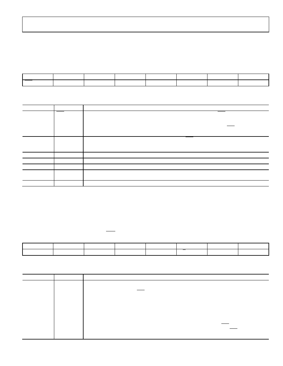
STATUS REGISTER (RS1, RS0 = 0, 0; POWER-ON/RESET = 0x8C)
The status register is an 8-bit read-only register. To access the ADC status register, the user must write to the communications register,
select the next operation to be a read, and load bits RS1 and RS0 with 0. Table 8 outlines the bit designations for the status register. SR0
through SR7 indicate the bit locations, SR denoting the bits are in the status register. SR7 denotes the first bit of the data stream. The
number in brackets indicates the power-on/reset default status of that bit.
SR7
SR6
SR5
SR4
SR3
SR2
SR1
SR0
RDY(1)
ERR(0)
0(0)
1(1)
WL(1)
CH1(0)
CH0(0)
Table 8. Status Register Bit Designations
Bit Location
Bit Name
Description
SR7
RDY
Ready bit for ADC. Cleared when data is written to the ADC data register. The RDY bit is set automatically
after the ADC data register has been read or a period of time before the data register is updated with a
new conversion result to indicate to the user not to read the conversion data. It is also set when the part
is placed in power-down mode. The end of a conversion is indicated by the DOUT/RDY pin also. This pin
can be used as an alternative to the status register for monitoring the ADC for conversion data.
SR6
ERR
ADC Error Bit. This bit is written to at the same time as the RDY bit. Set to indicate that the result written
to the ADC data register has been clamped to all 0s or all 1s. Error sources include overrange, under-
range. Cleared by a write operation to start a conversion.
SR5
0
This bit is automatically cleared.
SR4
0
This bit is automatically cleared.
SR3
1
This bit is automatically set.
SR2
1
This bit is automatically set if the device is an AD7791. It can be used to distinguish between the AD7791
and AD7790, in which the bit is cleared.
SR1–SR0
CH1–CH0
These bits indicate which channel is being converted by the ADC.
MODE REGISTER (RS1, RS0 = 0, 1; POWER-ON/RESET = 0x02)
The mode register is an 8-bit register from which data can be read or to which data can be written. This register is used to configure the
ADC for unipolar or bipolar mode, enable or disable the buffer, or place the device into power-down mode. Table 9 outlines the bit desig-
nations for the mode register. MR0 through MR7 indicate the bit locations, MR denoting the bits are in the mode register. MR7 denotes
the first bit of the data stream. The number in brackets indicates the power-on/reset default status of that bit. Any write to the setup regis-
ter resets the modulator and filter and sets the RDY bit.
MR7
MR6
MR5
MR4
MR3
MR2
MR1
MR0
MD1(0)
MD0(0)
0(0)
BO(0)
U/B(0)
BUF(1)
0(0)
Table 9. Mode Register Bit Designations
Bit Location
Bit Name
Description
MR7–MR6
MD1–MD0
Mode Select Bits. These bits select between continuous conversion mode, single conversion mode, and
standby mode. In continuous conversion mode, the ADC continuously performs conversions and places
the result in the data register. RDY goes low when a conversion is complete. The user can read these
conversions by placing the device in continuous read mode whereby the conversions are automatically
placed on the DOUT line when SCLK pulses are applied. Alternatively, the user can instruct the ADC to
output the conversion by writing to the communications register. After power-on, the first conversion is
available after a period 2/ fADC while subsequent conversions are available at a frequency of fADC. In single
conversion mode, the ADC is placed in power-down mode when conversions are not being performed.
When single conversion mode is selected, the ADC powers up and performs a single conversion, which
occurs after a period 2/fADC. The conversion result in placed in the data register, RDY goes low, and the
ADC returns to power-down mode. The conversion remains in the data register and RDY remains active
(low) until the data is read or another conversion is performed. See Table 10.
相关PDF资料 |
PDF描述 |
|---|---|
| VI-22Z-MY-B1 | CONVERTER MOD DC/DC 2V 20W |
| CS5529-ASZ | IC ADC 16BIT W/6BIT LATCH 20SSOP |
| VI-22Z-MW-B1 | CONVERTER MOD DC/DC 2V 40W |
| AD7798BRUZ | IC ADC 16BIT SIG-DEL 3CH 16TSSOP |
| VI-22T-MY-B1 | CONVERTER MOD DC/DC 6.5V 50W |
相关代理商/技术参数 |
参数描述 |
|---|---|
| AD7791BRMZ | 制造商:Analog Devices 功能描述:IC 16BIT ADC SMD 7791 MSOP10 |
| AD7791BRMZ-REEL | 功能描述:IC ADC 24BIT SIGMA-DELTA 10MSOP RoHS:是 类别:集成电路 (IC) >> 数据采集 - 模数转换器 系列:- 标准包装:1,000 系列:- 位数:16 采样率(每秒):45k 数据接口:串行 转换器数目:2 功率耗散(最大):315mW 电压电源:模拟和数字 工作温度:0°C ~ 70°C 安装类型:表面贴装 封装/外壳:28-SOIC(0.295",7.50mm 宽) 供应商设备封装:28-SOIC W 包装:带卷 (TR) 输入数目和类型:2 个单端,单极 |
| AD7792 | 制造商:AD 制造商全称:Analog Devices 功能描述:Low Power, 16/24-Bit Sigma-Delta ADC with Low-Noise In-Amp and Embedded Reference |
| AD7792_07 | 制造商:AD 制造商全称:Analog Devices 功能描述:3-Channel, Low Noise, Low Power, 16-/24-Bit ?£-?? ADC with On-Chip In-Amp and Reference |
| AD7792BRU | 功能描述:IC ADC 16BIT 3CH LP 16-TSSOP RoHS:否 类别:集成电路 (IC) >> 数据采集 - 模数转换器 系列:- 标准包装:1,000 系列:- 位数:16 采样率(每秒):45k 数据接口:串行 转换器数目:2 功率耗散(最大):315mW 电压电源:模拟和数字 工作温度:0°C ~ 70°C 安装类型:表面贴装 封装/外壳:28-SOIC(0.295",7.50mm 宽) 供应商设备封装:28-SOIC W 包装:带卷 (TR) 输入数目和类型:2 个单端,单极 |
发布紧急采购,3分钟左右您将得到回复。