- 您现在的位置:买卖IC网 > PDF目录10681 > AD7791BRMZ (Analog Devices Inc)IC ADC 24BIT BUFFERED LP 10MSOP PDF资料下载
参数资料
| 型号: | AD7791BRMZ |
| 厂商: | Analog Devices Inc |
| 文件页数: | 6/20页 |
| 文件大小: | 0K |
| 描述: | IC ADC 24BIT BUFFERED LP 10MSOP |
| 标准包装: | 50 |
| 位数: | 24 |
| 采样率(每秒): | 120 |
| 数据接口: | DSP,MICROWIRE?,QSPI?,串行,SPI? |
| 转换器数目: | 1 |
| 功率耗散(最大): | 230µW |
| 电压电源: | 单电源 |
| 工作温度: | -40°C ~ 105°C |
| 安装类型: | 表面贴装 |
| 封装/外壳: | 10-TFSOP,10-MSOP(0.118",3.00mm 宽) |
| 供应商设备封装: | 10-MSOP |
| 包装: | 管件 |
| 输入数目和类型: | 1 个差分,单极;1 个差分,双极 |
| 产品目录页面: | 779 (CN2011-ZH PDF) |
AD7791
Data Sheet
Rev. A | Page 14 of 20
ADC CIRCUIT INFORMATION
OVERVIEW
The AD7791 is a low power ADC that incorporates a ∑-Δ mod-
ulator, a buffer and on-chip digital filtering intended for the
measurement of wide dynamic range, low frequency signals
such as those in pressure transducers, weigh scales, and temper-
ature measurement applications.
The part has one differential input that can be buffered or
unbuffered. Buffering the input channel means that the part can
accommodate significant source impedances on the analog
input and that R, C filtering (for noise rejection or RFI reduc-
tion) can be placed on the analog input, if required. The device
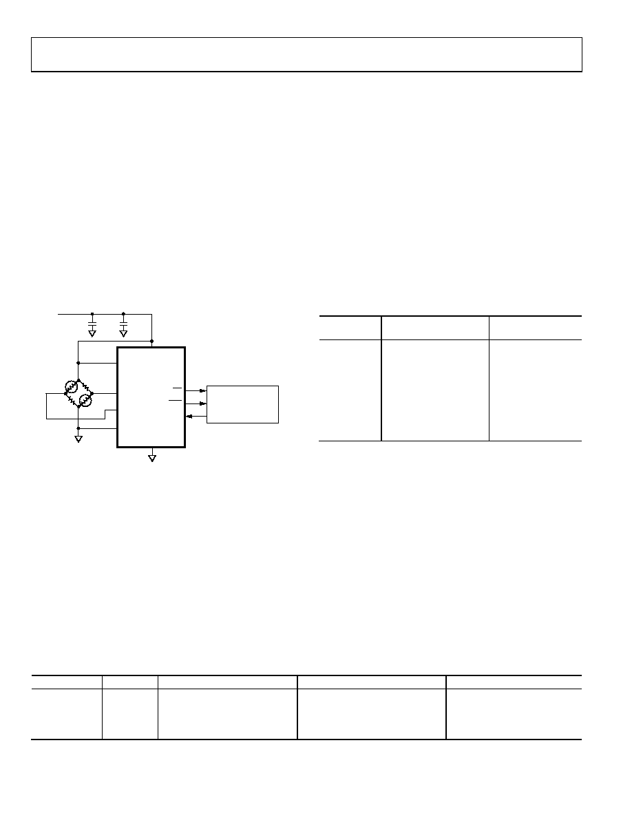
requires an external reference of 2.5 nominal. Figure 12 shows
the basic connections required to operate the part.
04227-0-006
IN+
10
F
0.1
F
IN–
OUT–
POWER
SUPPLY
OUT+
REFIN(+)
CS
DOUT/RDY
SCLK
VDD
GND
AIN(+)
AIN(–)
REFIN(–)
AD7791
MICROCONTROLLER
Figure 12. Basic Connection Diagram
The output rate of the AD7791 (fADC) is user programmable
with the settling time equal to 2 × tADC. Normal mode rejection
is the major function of the digital filter. Table 12 lists the avail-
able output rates from the AD7791. Simultaneous 50 Hz and
60 Hz rejection is optimized when the update rate equals
16.6 Hz as notches are placed at both 50 Hz and 60 Hz with this
update rate (see Figure 6).
NOISE PERFORMANCE
Table 13 shows the output rms noise, rms resolution, and peak-
to-peak resolution (rounded to the nearest 0.5 LSB) for the
different update rates and input ranges for the AD7791. The
numbers given are for the bipolar input range with a reference
of 2.5 V. These numbers are typical and generated with a differ-
ential input voltage of 0 V. The peak-to-peak resolution figures
represent the resolution for which there will be no code flicker
within a six-sigma limit. The output noise comes from two
sources. The first is the electrical noise in the semiconductor
devices (device noise) used in the implementation of the modu-
lator. The second is quantization noise, which is added when
the analog input is converted into the digital domain. The de-
vice noise is at a low level and is independent of frequency. The
quantization noise starts at an even lower level but rises rapidly
with increasing frequency to become the dominant noise
source.
Table 13. Typical Peak-to-Peak Resolution (Effective
Resolution) vs. Update Rate
Update
Rate
Peak-toPeak Resolu-
tion
Effective Resolu-
tion
9.5
19.5
22
13.3
19
21.5
16.7
19
21.5
16.6
19
21.5
20
18.5
21
33.3
17.5
20
100
14.5
17
120
14
16.5
REDUCED CURRENT MODES
The AD7791 has a current consumption of 160 μA maximum
when operated with a 5 V power supply, the buffer enabled, and
the clock operating at its maximum speed. The clock frequency
can be divided by a factor of 2, 4, or 8 before being applied to
the modulator and filter, resulting in a reduction in the current
consumption of the AD7791. Bits CDIV1 and CDIV0 in the filter
register are used to enter these low power modes (see Table 14).
When the internal clock is reduced, the update rate will also be
reduced. For example, if the filter bits are set to give an update
rate of 16.6 Hz when the AD7791 is operated in full power
mode, the update rate will equal 8.3 Hz in divide by 2 mode. In
the low power modes, there may be some degradation in the
ADC performance.
Table 14. Low Power Mode Selection
CDIV[1:0]
Clock
Typ Current, Buffered (μA)
Typ Current, Unbuffered (μA)
50 Hz/60 Hz Rejection (dB)
00
1
146
75
65
10
1/2
87
45
64
10
1/4
56
30
75
11
1/8
41
25
86
相关PDF资料 |
PDF描述 |
|---|---|
| VI-22Z-MY-B1 | CONVERTER MOD DC/DC 2V 20W |
| CS5529-ASZ | IC ADC 16BIT W/6BIT LATCH 20SSOP |
| VI-22Z-MW-B1 | CONVERTER MOD DC/DC 2V 40W |
| AD7798BRUZ | IC ADC 16BIT SIG-DEL 3CH 16TSSOP |
| VI-22T-MY-B1 | CONVERTER MOD DC/DC 6.5V 50W |
相关代理商/技术参数 |
参数描述 |
|---|---|
| AD7791BRMZ | 制造商:Analog Devices 功能描述:IC 16BIT ADC SMD 7791 MSOP10 |
| AD7791BRMZ-REEL | 功能描述:IC ADC 24BIT SIGMA-DELTA 10MSOP RoHS:是 类别:集成电路 (IC) >> 数据采集 - 模数转换器 系列:- 标准包装:1,000 系列:- 位数:16 采样率(每秒):45k 数据接口:串行 转换器数目:2 功率耗散(最大):315mW 电压电源:模拟和数字 工作温度:0°C ~ 70°C 安装类型:表面贴装 封装/外壳:28-SOIC(0.295",7.50mm 宽) 供应商设备封装:28-SOIC W 包装:带卷 (TR) 输入数目和类型:2 个单端,单极 |
| AD7792 | 制造商:AD 制造商全称:Analog Devices 功能描述:Low Power, 16/24-Bit Sigma-Delta ADC with Low-Noise In-Amp and Embedded Reference |
| AD7792_07 | 制造商:AD 制造商全称:Analog Devices 功能描述:3-Channel, Low Noise, Low Power, 16-/24-Bit ?£-?? ADC with On-Chip In-Amp and Reference |
| AD7792BRU | 功能描述:IC ADC 16BIT 3CH LP 16-TSSOP RoHS:否 类别:集成电路 (IC) >> 数据采集 - 模数转换器 系列:- 标准包装:1,000 系列:- 位数:16 采样率(每秒):45k 数据接口:串行 转换器数目:2 功率耗散(最大):315mW 电压电源:模拟和数字 工作温度:0°C ~ 70°C 安装类型:表面贴装 封装/外壳:28-SOIC(0.295",7.50mm 宽) 供应商设备封装:28-SOIC W 包装:带卷 (TR) 输入数目和类型:2 个单端,单极 |
发布紧急采购,3分钟左右您将得到回复。