- 您现在的位置:买卖IC网 > PDF目录8616 > AD7808BRZ-REEL (Analog Devices Inc)IC DAC 10BIT OCTAL SRL 24-SOIC PDF资料下载
参数资料
| 型号: | AD7808BRZ-REEL |
| 厂商: | Analog Devices Inc |
| 文件页数: | 6/28页 |
| 文件大小: | 0K |
| 描述: | IC DAC 10BIT OCTAL SRL 24-SOIC |
| 产品培训模块: | Data Converter Fundamentals DAC Architectures |
| 标准包装: | 1,000 |
| 设置时间: | 1.5µs |
| 位数: | 10 |
| 数据接口: | 串行 |
| 转换器数目: | 4 |
| 电压电源: | 模拟和数字 |
| 功率耗散(最大): | 99mW |
| 工作温度: | -40°C ~ 85°C |
| 安装类型: | 表面贴装 |
| 封装/外壳: | 24-SOIC(0.295",7.50mm 宽) |
| 供应商设备封装: | 24-SOIC W |
| 包装: | 带卷 (TR) |
| 输出数目和类型: | 8 电压,双极 |
| 采样率(每秒): | 667k |
第1页第2页第3页第4页第5页当前第6页第7页第8页第9页第10页第11页第12页第13页第14页第15页第16页第17页第18页第19页第20页第21页第22页第23页第24页第25页第26页第27页第28页
AD7804/AD7805/AD7808/AD7809
REV. A
–14–
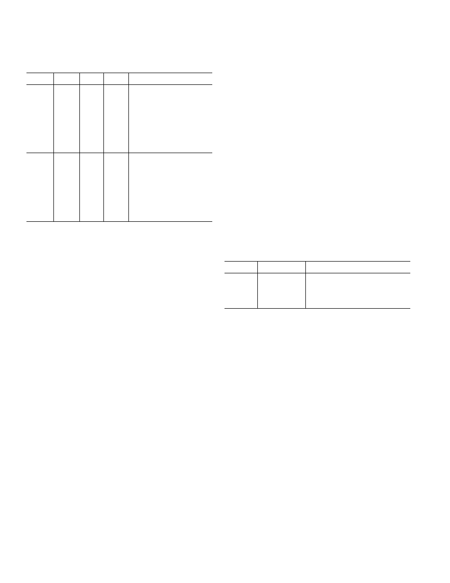
Table IVb. AD7809 DAC Data/Control Register
Selection Table
MODE
A2
A1
A0
Function Selected
0
DAC A Control Register
0
1
DAC B Control Register
0
1
0
DAC C Control Register
0
1
DAC D Control Register
0
1
0
DAC E Control Register
0
1
0
1
DAC F Control Register
0
1
0
DAC G Control Register
0
1
DAC H Control Register
1
0
DAC A Data Register
1
0
1
DAC B Data Register
1
0
1
0
DAC C Data Register
1
0
1
DAC D Data Register
1
0
DAC E Data Register
1
0
1
DAC F Data Register
1
0
DAC G Data Register
1
DAC H Data Register
AD7805/AD7809 SYSTEM OR CHANNEL CONTROL
REGISTER SELECTION
MD0
0
This enables writing to the system control register.
The contents of this are shown in Figure 12. Mode
must be low to access this control register.
1
This enables writing to the channel control register.
The contents of this are shown in Figure 13. Mode
must also be low to access this control register.
AD7805/AD7809 SYSTEM CONTROL REGISTER
The bits in this register allow control over all DACs in the pack-
age. The control bits include data format (
10/8), power down
(
PD), DAC input coding select (BIN/COMP), system standby
(SSTBY) and a system clear (SCLR). The function of these bits
is as follows:
Data Format
10/8
0
10-bit parallel loading structure.
1
Byte loading structure. (8+2 loading).
Input Coding
BIN/
COMP
0
Twos complement coding.
1
Offset Binary Coding.
Power Down
PD
0
Complete power-down of device.
1
Normal operation (default on power-up).
System Standby
SSTBY
0
Normal operation.
1
All DACs in the package put in standby mode (default
on power-up).
System Clear
SCLR
0
Normal operation.
1
All DACs in the package are cleared to a known state
depending on the coding scheme selected. The SCLR bit
clears the Main DACs only; the Sub DACs are unaf-
fected by the system clear function. The main DAC is
cleared to different levels depending on the coding
scheme. With offset binary coding the Main DAC output
is cleared to the bottom of the transfer function VBIAS/16.
With twos complement coding the Main DAC output is
cleared to midscale VBIAS. The channel output will be the
sum of the Main DAC and Sub DAC contributions.
AD7805/AD7809 CHANNEL CONTROL REGISTER
This register allows the user to have control over individual
DACs in the package. The control bits in this register include
multiplexer output selection (MX1 and MX0), Main or Sub
DAC selection (
MAIN/SUB), standby (STBY) and individual
DAC clear (CLR). The function of these bits is as follows.
Multiplexer Selection (MX1, MX0)
Table V shows the VBIAS selection using MX1 and MX0 bits in
the channel control register.
Table V. VBIAS Selection Table
MX1
MX0
VBIAS
00
VDD/2 (Default on Power-Up)
0
1
INTERNAL VREF
1
0
REFIN
1
Undetermined
Main DAC or Sub DAC Selection
MAIN/SUB
0
Writing a 0 to this bit means that the data in the next
data register write is transferred to the selected Main
DAC.
1
Writing a 1 to this bit means that the data in the next
data register write is transferred to the selected Sub DAC.
This applies to the 10-bit parallel load feature. In byte
load mode, (Figure 15) DB0 selects the Main or Sub
DAC data registers.
Standby
STBY
0
Places the selected DAC and its associated linear cir-
cuitry in Standby Mode.
1
Normal operation (default on power-up).
Clear
CLR
0
Normal operation.
1
Clears the output of the selected Main DAC to one
of two conditions depending on the input coding se-
lected. With offset binary coding the Main DAC out-
put is cleared to the bottom of the transfer function,
VBIAS/16 and with twos complement coding the Main
DAC output is cleared to midscale VBIAS. The Sub
DAC is unaffected by a clear operation. An
LDAC
signal has to be applied to the DAC for a channel clear
to be implemented.
相关PDF资料 |
PDF描述 |
|---|---|
| VI-J6J-MW-S | CONVERTER MOD DC/DC 36V 100W |
| LT1567IMS8 | IC BLOCK BUILD FLTR LONOIS 8MSOP |
| VI-J6B-MW-S | CONVERTER MOD DC/DC 95V 100W |
| VI-25X-IV-F3 | CONVERTER MOD DC/DC 5.2V 150W |
| VI-25X-IV-F2 | CONVERTER MOD DC/DC 5.2V 150W |
相关代理商/技术参数 |
参数描述 |
|---|---|
| AD7808BST | 制造商:AD 制造商全称:Analog Devices 功能描述:+3.3 V to +5 V Quad/Octal 10-Bit DACs(300.12 k) |
| AD7809 | 制造商:AD 制造商全称:Analog Devices 功能描述:+3.3 V to +5 V Quad/Octal 10-Bit DACs |
| AD7809BST | 制造商:Analog Devices 功能描述:DAC 8-CH 10-bit 44-Pin TQFP 制造商:Rochester Electronics LLC 功能描述:OCTAL 10-BIT PARALLEL DAC I.C. - Bulk 制造商:Analog Devices 功能描述:IC 10-BIT DAC |
| AD7809BST-REEL | 制造商:Analog Devices 功能描述:DAC 8-CH 10-bit 44-Pin TQFP T/R |
发布紧急采购,3分钟左右您将得到回复。