- 您现在的位置:买卖IC网 > PDF目录8616 > AD7808BRZ-REEL (Analog Devices Inc)IC DAC 10BIT OCTAL SRL 24-SOIC PDF资料下载
参数资料
| 型号: | AD7808BRZ-REEL |
| 厂商: | Analog Devices Inc |
| 文件页数: | 8/28页 |
| 文件大小: | 0K |
| 描述: | IC DAC 10BIT OCTAL SRL 24-SOIC |
| 产品培训模块: | Data Converter Fundamentals DAC Architectures |
| 标准包装: | 1,000 |
| 设置时间: | 1.5µs |
| 位数: | 10 |
| 数据接口: | 串行 |
| 转换器数目: | 4 |
| 电压电源: | 模拟和数字 |
| 功率耗散(最大): | 99mW |
| 工作温度: | -40°C ~ 85°C |
| 安装类型: | 表面贴装 |
| 封装/外壳: | 24-SOIC(0.295",7.50mm 宽) |
| 供应商设备封装: | 24-SOIC W |
| 包装: | 带卷 (TR) |
| 输出数目和类型: | 8 电压,双极 |
| 采样率(每秒): | 667k |
第1页第2页第3页第4页第5页第6页第7页当前第8页第9页第10页第11页第12页第13页第14页第15页第16页第17页第18页第19页第20页第21页第22页第23页第24页第25页第26页第27页第28页
AD7804/AD7805/AD7808/AD7809
REV. A
–16–
POWER-DOWN AND STANDBY FUNCTIONS
There are two distinct low power modes on the device, power-
down mode and standby mode. When in power-down mode all
circuitry including the reference are put into low power mode
and power dissipation from the package is at its minimum.
A2
A1
A0
SYSTEM
PD
SYSTEM
STBY
ONLY ONE DAC SHOWN FOR CLARITY
ADDR
DECODER
STANDBY
INT
REFERENCE
CHANNEL
STBY
STANDBY
MAIN & SUB
DAC
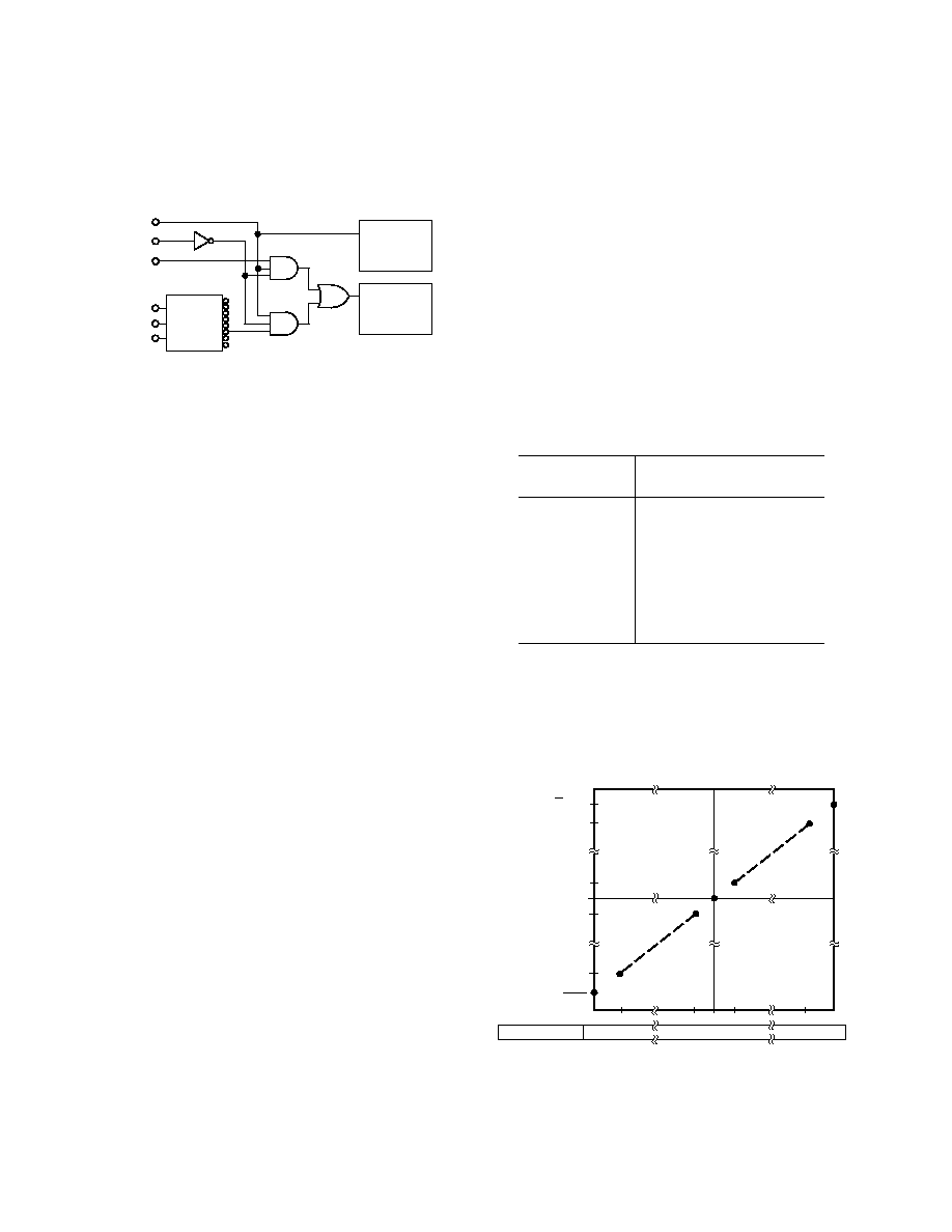
Figure 21. Implementation of Power-Down and Standby
Functions
The standby functions allow either the selected DAC or all DACs
in the package to be put into low power mode. The reference is
not switched off when any of the standby functions are invoked.
The
PD bit in the system control register is used to shut down
the complete device. With a 0 in this position the reference and all
DACs are put into low power mode. Writing a 1 to this bit puts the
part in the normal operating mode. When in power-down mode
the contents of all registers are retained and are valid when the
device is taken out of power down. The SSTBY bit which resides
in the system control register can be used to put all DACs and
their associated linear circuitry into standby mode, the SSTBY
function does not power down the reference. The
STBY bit in
the channel control register can be used to put a selected DAC
and its associated linear circuitry into standby mode. Figure 18
shows a simplified diagram of how the power-down and standby
functions are implemented for a single DAC in the package.
LDAC FUNCTION
LDAC input is a logic input that allows all DAC registers to be
simultaneously updated with the contents of the DAC data
registers.
LDAC input has two operating modes, a synchronous
mode and an asynchronous mode. The
LDAC input condition is
sampled on the sixteenth falling edge on the AD7804/AD7808 and
is sampled on the rising edge of write on the AD7805/AD7809. If
LDAC is low on the sixteenth falling clock edge or on the rising
edge of
WR, an automatic or synchronous update will take place.
LDAC input can be tied permanently low or have timing similar
to that of the data inputs to operate in the synchronous mode.
If
LDAC is high during the sample period, the AD7804/AD7805/
AD7808/AD7809 assumes an asynchronous update. When in
the asynchronous mode, an
LDAC setup time has to be allowed
following the sixteenth falling clock edge or the rising edge of
WR before the LDAC can be activated.
ANALOG OUTPUTS
The AD7804 and AD7805 DACs contain four independent
voltage output Main DACs with 10-bit resolution. The AD7808
and AD7809 contain eight independent voltage output main
DACs with 10-bit resolution. Each Main DAC has an associ-
ated Sub DAC with 8-bit resolution which can be used to offset
the complete transfer function of the Main DAC around the
VBIAS point. These DACs produce an output voltage in the form
of VBIAS
±V
SWING where VSWING is 15/16 of VBIAS.
The digital input code to these DACs can be in twos comple-
ment or offset binary form. All DACs will be configured with
the same input coding scheme which is programmed through
the system control register. The default condition on power-up
is for offset binary coding.
TWOS COMPLEMENT CODING
Table VI shows the twos complement transfer function for the
Main DAC.
Table VI. Twos Complement Code Table for Main DAC
Digital Input
Analog Output
MSB
... LSB
0111111111
VBIAS(1+1.875
× 511/1024)
0111111110
VBIAS(1+1.875
× 510/1024)
0000000001
VBIAS(1+1.875
× 1/1024)
0000000000
VBIAS
1111111111
VBIAS(1–1.875
× 1/1024)
1000000001
VBIAS(1–1.875 × 511/1024)
1000000000
VBIAS(1–1.875 × 512/1024)
Figure 22 shows the Main DAC transfer function for twos
complement coding. Any Main DAC output voltage can be
expressed as:
VOUT' = VBIAS + 1.875
× V
BIAS
× NA/1024
where NA is the decimal equivalent of the twos complement
input code. NA ranges from –512 to +511.
VBIAS
DAC
OUTPUT
VOLTAGE
200
201
DAC INPUT CODE
3FF 000 001
1FE
1FF
VBIAS
16
31
16 VBIAS
Figure 22. Main DAC Output Voltage vs. DAC Input Codes
(HEX) for Twos Complement Coding
相关PDF资料 |
PDF描述 |
|---|---|
| VI-J6J-MW-S | CONVERTER MOD DC/DC 36V 100W |
| LT1567IMS8 | IC BLOCK BUILD FLTR LONOIS 8MSOP |
| VI-J6B-MW-S | CONVERTER MOD DC/DC 95V 100W |
| VI-25X-IV-F3 | CONVERTER MOD DC/DC 5.2V 150W |
| VI-25X-IV-F2 | CONVERTER MOD DC/DC 5.2V 150W |
相关代理商/技术参数 |
参数描述 |
|---|---|
| AD7808BST | 制造商:AD 制造商全称:Analog Devices 功能描述:+3.3 V to +5 V Quad/Octal 10-Bit DACs(300.12 k) |
| AD7809 | 制造商:AD 制造商全称:Analog Devices 功能描述:+3.3 V to +5 V Quad/Octal 10-Bit DACs |
| AD7809BST | 制造商:Analog Devices 功能描述:DAC 8-CH 10-bit 44-Pin TQFP 制造商:Rochester Electronics LLC 功能描述:OCTAL 10-BIT PARALLEL DAC I.C. - Bulk 制造商:Analog Devices 功能描述:IC 10-BIT DAC |
| AD7809BST-REEL | 制造商:Analog Devices 功能描述:DAC 8-CH 10-bit 44-Pin TQFP T/R |
发布紧急采购,3分钟左右您将得到回复。