- 您现在的位置:买卖IC网 > PDF目录9787 > AD7811YRUZ-REEL (Analog Devices Inc)IC ADC 10BIT 4CHAN SRL 16-TSSOP PDF资料下载
参数资料
| 型号: | AD7811YRUZ-REEL |
| 厂商: | Analog Devices Inc |
| 文件页数: | 3/24页 |
| 文件大小: | 0K |
| 描述: | IC ADC 10BIT 4CHAN SRL 16-TSSOP |
| 产品变化通告: | Product Discontinuance 27/Oct/2011 |
| 标准包装: | 2,500 |
| 位数: | 10 |
| 采样率(每秒): | 350k |
| 数据接口: | DSP,串行 |
| 转换器数目: | 1 |
| 功率耗散(最大): | 10.5mW |
| 电压电源: | 单电源 |
| 工作温度: | -40°C ~ 105°C |
| 安装类型: | 表面贴装 |
| 封装/外壳: | 16-TSSOP(0.173",4.40mm 宽) |
| 供应商设备封装: | 16-TSSOP |
| 包装: | 带卷 (TR) |
| 输入数目和类型: | 4 个单端,单极;3 个伪差分,单极 |
AD7811/AD7812
–11–
REV. B
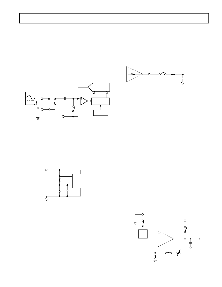
An example of the pseudo differential scheme using the AD7811
is shown in Figure 6. The relevant bits in the AD7811 Control
Register are set as follows DIF/
SGL = 1, CH1 = CH2 = 0, i.e.,
VIN1 pseudo differential with respect to VIN2. The signal is
applied to VIN1 but in the pseudo differential scheme the sam-
pling capacitor is connected to VIN2 during conversion and not
AGND as described in the Converter Operation section. This
input scheme can be used to remove offsets that exist in a sys-
tem. For example, if a system had an offset of 0.5 V the offset
could be applied to VIN2 and the signal applied to VIN1. This has
the effect of offsetting the input span by 0.5 V. It is only pos-
sible to offset the input span when the reference voltage is less
than VDD–OFFSET.
VIN1
VDD/3
COMPARATOR
CONTROL
LOGIC
CLOCK
OSC
CONVERSION
PHASE
VOFFSET
SAMPLING
CAPACITOR
VIN+
VIN–
VIN2
VIN1
CHARGE
REDISTRIBUTION
DAC
VOFFSET
Figure 6. Pseudo Differential Input Scheme
When using the pseudo differential input scheme the signal on
VIN2 must not vary by more than a 1/2 LSB during the conver-
sion process. If the signal on VIN2 varies during conversion, the
conversion result will be incorrect. In single-ended mode the
sampling capacitor is always connected to AGND during con-
version. Figure 7 shows the AD7811/AD7812 pseudo differen-
tial input being used to make a unipolar dc current measurement.
A sense resistor is used to convert the current to a voltage and
the voltage is applied to the differential input as shown.
RL
RSENSE
AD7811/
AD7812
VIN+
VIN–
VDD
Figure 7. DC Current Measurement Scheme
DC Acquisition Time
The ADC starts a new acquisition phase at the end of a conver-
sion and ends on the falling edge of the
CONVST signal. At the
end of a conversion a settling time is associated with the sam-
pling circuit. This settling time lasts approximately 100 ns. The
analog signal on VIN+ is also being acquired during this settling
time. Therefore, the minimum acquisition time needed is
approximately 100 ns.
Figure 8 shows the equivalent charging circuit for the sampling
capacitor when the ADC is in its acquisition phase. R2 repre-
sents the source impedance of a buffer amplifier or resistive
network; R1 is an internal multiplexer resistance, and C1 is the
sampling capacitor. During the acquisition phase the sampling
capacitor must be charged to within a 1/2 LSB of its final value.
The time it takes to charge the sampling capacitor (TCHARGE) is
given by the following formula:
TCHARGE = 7.6
× (R2 + 125 ) × 3.5 pF
C1
3.5pF
VIN+
R1
125
R2
SAMPLING
CAPACITOR
Figure 8. Equivalent Sampling Circuit
For small values of source impedance, the settling time associ-
ated with the sampling circuit (100 ns) is, in effect, the acquisi-
tion time of the ADC. For example, with a source impedance
(R2) of 10
the charge time for the sampling capacitor is
approximately 4 ns. The charge time becomes significant for
source impedances of 2 k
and greater.
AC Acquisition Time
In ac applications it is recommended to always buffer analog
input signals. The source impedance of the drive circuitry must
be kept as low as possible to minimize the acquisition time of
the ADC. Large values of source impedance will cause the THD
to degrade at high throughput rates. In addition, better perfor-
mance can generally be achieved by using an External 1 nF
capacitor on V
IN.
ON-CHIP REFERENCE
The AD7811 and AD7812 have an on-chip 2.5 V reference
circuit. The schematic in Figure 9 shows how the reference
circuit is implemented. A 1.23 V bandgap reference is gained up
to provide a 2.5 V
± 2% reference voltage. The on-chip refer-
ence is not available externally (SW2 is open). An external refer-
ence (1.2 V to VDD) can be applied at the VREF pin. However in
order to use an external reference the EXTREF bit in the con-
trol register (Bit 0) must first be set to a Logic 1. When EXTREF
is set to a Logic 1 SW2 will close, SW3 will open and the ampli-
fier will power down. This will reduce the current consumption
of the part by about 1 mA. It is possible to use two different
reference voltages by selecting the on-chip reference or external
reference.
7pF
2.5V
EXTERNAL
CAPACITOR
1.23V
VREF
CREF
AGND
SW3
SW2
SW1
Figure 9. On-Chip Reference Circuitry
C
相关PDF资料 |
PDF描述 |
|---|---|
| VI-BT4-MW-F3 | CONVERTER MOD DC/DC 48V 100W |
| VE-2NX-IU-F4 | CONVERTER MOD DC/DC 5.2V 200W |
| VI-BT4-MW-F2 | CONVERTER MOD DC/DC 48V 100W |
| V150B48M150BG | CONVERTER MOD DC/DC 48V 150W |
| V150B48M150BF3 | CONVERTER MOD DC/DC 48V 150W |
相关代理商/技术参数 |
参数描述 |
|---|---|
| AD7811YRUZ-REEL7 | 功能描述:IC ADC 10BIT 4CHAN SRL 16-TSSOP RoHS:是 类别:集成电路 (IC) >> 数据采集 - 模数转换器 系列:- 标准包装:2,500 系列:- 位数:16 采样率(每秒):15 数据接口:MICROWIRE?,串行,SPI? 转换器数目:1 功率耗散(最大):480µW 电压电源:单电源 工作温度:-40°C ~ 85°C 安装类型:表面贴装 封装/外壳:38-WFQFN 裸露焊盘 供应商设备封装:38-QFN(5x7) 包装:带卷 (TR) 输入数目和类型:16 个单端,双极;8 个差分,双极 配用:DC1011A-C-ND - BOARD DELTA SIGMA ADC LTC2494 |
| AD7811YRZ | 功能描述:IC ADC 10BIT 4-CH 2.7V 16-SOIC RoHS:是 类别:集成电路 (IC) >> 数据采集 - 模数转换器 系列:- 其它有关文件:TSA1204 View All Specifications 标准包装:1 系列:- 位数:12 采样率(每秒):20M 数据接口:并联 转换器数目:2 功率耗散(最大):155mW 电压电源:模拟和数字 工作温度:-40°C ~ 85°C 安装类型:表面贴装 封装/外壳:48-TQFP 供应商设备封装:48-TQFP(7x7) 包装:Digi-Reel® 输入数目和类型:4 个单端,单极;2 个差分,单极 产品目录页面:1156 (CN2011-ZH PDF) 其它名称:497-5435-6 |
| AD7811YRZ-REEL | 功能描述:IC ADC 10BIT 4CHAN SRL 16SOIC RoHS:是 类别:集成电路 (IC) >> 数据采集 - 模数转换器 系列:- 标准包装:2,500 系列:- 位数:16 采样率(每秒):15 数据接口:MICROWIRE?,串行,SPI? 转换器数目:1 功率耗散(最大):480µW 电压电源:单电源 工作温度:-40°C ~ 85°C 安装类型:表面贴装 封装/外壳:38-WFQFN 裸露焊盘 供应商设备封装:38-QFN(5x7) 包装:带卷 (TR) 输入数目和类型:16 个单端,双极;8 个差分,双极 配用:DC1011A-C-ND - BOARD DELTA SIGMA ADC LTC2494 |
| AD7811YRZ-REEL7 | 功能描述:IC ADC 10BIT 4CHAN SRL 16SOIC RoHS:是 类别:集成电路 (IC) >> 数据采集 - 模数转换器 系列:- 产品培训模块:Lead (SnPb) Finish for COTS Obsolescence Mitigation Program 标准包装:2,500 系列:- 位数:12 采样率(每秒):3M 数据接口:- 转换器数目:- 功率耗散(最大):- 电压电源:- 工作温度:- 安装类型:表面贴装 封装/外壳:SOT-23-6 供应商设备封装:SOT-23-6 包装:带卷 (TR) 输入数目和类型:- |
| AD7812 | 制造商:AD 制造商全称:Analog Devices 功能描述:+2.7 V to +5.5 V, 350 kSPS, 10-Bit 4-/8-Channel Sampling ADCs |
发布紧急采购,3分钟左右您将得到回复。