- 您现在的位置:买卖IC网 > PDF目录9787 > AD7811YRUZ-REEL (Analog Devices Inc)IC ADC 10BIT 4CHAN SRL 16-TSSOP PDF资料下载
参数资料
| 型号: | AD7811YRUZ-REEL |
| 厂商: | Analog Devices Inc |
| 文件页数: | 7/24页 |
| 文件大小: | 0K |
| 描述: | IC ADC 10BIT 4CHAN SRL 16-TSSOP |
| 产品变化通告: | Product Discontinuance 27/Oct/2011 |
| 标准包装: | 2,500 |
| 位数: | 10 |
| 采样率(每秒): | 350k |
| 数据接口: | DSP,串行 |
| 转换器数目: | 1 |
| 功率耗散(最大): | 10.5mW |
| 电压电源: | 单电源 |
| 工作温度: | -40°C ~ 105°C |
| 安装类型: | 表面贴装 |
| 封装/外壳: | 16-TSSOP(0.173",4.40mm 宽) |
| 供应商设备封装: | 16-TSSOP |
| 包装: | 带卷 (TR) |
| 输入数目和类型: | 4 个单端,单极;3 个伪差分,单极 |
AD7811/AD7812
–15–
REV. B
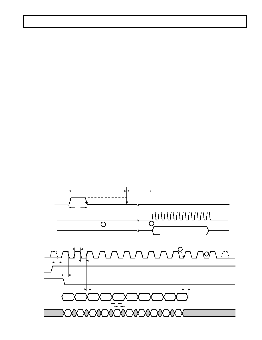
enter during automatic power-down. These modes are discussed
in the Power-Up Times section of this data sheet. The timing
diagram in Figure 17 shows how to operate the part in Mode 2.
If the AD7811/AD7812 is powered down, the rising edge of the
CONVST pulse causes the part to power-up. Once the part
has powered up (~1.5
s after the rising edge of CONVST)
the
CONVST signal is brought low and a conversion is initiated
on this falling edge of the
CONVST signal. The conversion
takes 2.3
s and after this time the conversion result is latched
into the serial shift register and the part powers down. There-
fore, when the part is operated in Mode 2 the effective conver-
sion time is equal to the power-up time (1.5
s) and the SAR
conversion time (2.3
s).
NOTE: Although the AD7811 and AD7812 take 1.5
s to
power up after the rising edge of
CONVST, it is not necessary
to leave
CONVST high for 1.5
s after the rising edge before
bringing it low to initiate a conversion. If the
CONVST signal
goes low before 1.5
s in time has elapsed, then the power-up
time is timed out internally and a conversion is then initiated.
Hence the AD7811 and AD7812 are guaranteed to have always
powered-up before a conversion is initiated, even if the
CONVST
pulsewidth is <1.5
s. If the CONVST pulsewidth is > 1.5 s,
then a conversion is initiated on the falling edge.
As in the case of Mode 1 operation, the rising edge of the first
SCLK after the rising edge of RFS enables the serial port of the
AD7811 and AD7812 (see Serial Interface section). If a serial
read is initiated soon after this rising edge (Point “A”), i.e.,
before the end of the conversion, the result of the previous con-
version is shifted out on pin DOUT. In order to read the result
of the current conversion, the user must wait at least 2.3
s after
power-up or at least 2.3
s after the falling edge of CONVST,
(Point “B”), whichever occurs latest before initiating a serial
read. The serial port of the AD7811 and AD7812 is still func-
tional even though the devices have been powered down.
Because it is possible to do a serial read from the part while it is
powered down, the AD7811 and AD7812 are powered up only
to do the conversion and are immediately powered down at the
end of a conversion. This significantly improves the power
consumption of the part at slower throughput rates—see Power
vs. Throughput section.
SERIAL INTERFACE
The serial interface of the AD7811 and AD7812 consists of five
wires, a serial clock input, SCLK, receive data to clock syn-
chronization input RFS, transmit data to clock synchronization
input TFS, a serial data output, DOUT, and a serial data
input, DIN, (see Figure 18). The serial interface is designed to
allow easy interfacing to most microcontrollers and DSPs,
e.g., PIC16C, PIC17C, QSPI, SPI, DSP56000, TMS320
and ADSP-21xx, without the need for any gluing logic. When
interfacing to the 8051, the SCLK must be inverted. The
Microprocessor/Microcontroller Interface section explains
how to interface to some popular DSPs and microcontrollers.
Figure 18 shows the timing diagram for a serial read and write
to the AD7811 and AD7812. The serial interface works with
both a continuous and a noncontinuous serial clock. The rising
edge of RFS and falling edge of TFS resets a counter that
counts the number of serial clocks to ensure the correct number
of bits are shifted in and out of the serial shift registers. Once
the correct number of bits have been shifted in and out, the
SCLK is ignored. In order for another serial transfer to take
place the counter must be reset by the active edges of TFS and
CURRENT CONVERSION
RESULT
A
B
t
POWER-UP
CONVST
DOUT
SCLK
1.5 s
t
1
t
2
Figure 17. Mode 2 Operation Timing Diagram
A
B
DIN
DB9
DB8
DB9
DB7
DB8
DB7
DB6
DB5
DB4
DB3
DB0
SCLK
RFS
DOUT
t
3
t
7
t
4
t
10
DB1
DB2
1
13
12
11
10
9
8
7
6
5
4
3
2
TFS
t
8
t
9
t
5
t
6
DB6
DB5
DB4
DB3
DB2
DB1
DB0
Figure 18. Serial Interface Timing Diagram
C
相关PDF资料 |
PDF描述 |
|---|---|
| VI-BT4-MW-F3 | CONVERTER MOD DC/DC 48V 100W |
| VE-2NX-IU-F4 | CONVERTER MOD DC/DC 5.2V 200W |
| VI-BT4-MW-F2 | CONVERTER MOD DC/DC 48V 100W |
| V150B48M150BG | CONVERTER MOD DC/DC 48V 150W |
| V150B48M150BF3 | CONVERTER MOD DC/DC 48V 150W |
相关代理商/技术参数 |
参数描述 |
|---|---|
| AD7811YRUZ-REEL7 | 功能描述:IC ADC 10BIT 4CHAN SRL 16-TSSOP RoHS:是 类别:集成电路 (IC) >> 数据采集 - 模数转换器 系列:- 标准包装:2,500 系列:- 位数:16 采样率(每秒):15 数据接口:MICROWIRE?,串行,SPI? 转换器数目:1 功率耗散(最大):480µW 电压电源:单电源 工作温度:-40°C ~ 85°C 安装类型:表面贴装 封装/外壳:38-WFQFN 裸露焊盘 供应商设备封装:38-QFN(5x7) 包装:带卷 (TR) 输入数目和类型:16 个单端,双极;8 个差分,双极 配用:DC1011A-C-ND - BOARD DELTA SIGMA ADC LTC2494 |
| AD7811YRZ | 功能描述:IC ADC 10BIT 4-CH 2.7V 16-SOIC RoHS:是 类别:集成电路 (IC) >> 数据采集 - 模数转换器 系列:- 其它有关文件:TSA1204 View All Specifications 标准包装:1 系列:- 位数:12 采样率(每秒):20M 数据接口:并联 转换器数目:2 功率耗散(最大):155mW 电压电源:模拟和数字 工作温度:-40°C ~ 85°C 安装类型:表面贴装 封装/外壳:48-TQFP 供应商设备封装:48-TQFP(7x7) 包装:Digi-Reel® 输入数目和类型:4 个单端,单极;2 个差分,单极 产品目录页面:1156 (CN2011-ZH PDF) 其它名称:497-5435-6 |
| AD7811YRZ-REEL | 功能描述:IC ADC 10BIT 4CHAN SRL 16SOIC RoHS:是 类别:集成电路 (IC) >> 数据采集 - 模数转换器 系列:- 标准包装:2,500 系列:- 位数:16 采样率(每秒):15 数据接口:MICROWIRE?,串行,SPI? 转换器数目:1 功率耗散(最大):480µW 电压电源:单电源 工作温度:-40°C ~ 85°C 安装类型:表面贴装 封装/外壳:38-WFQFN 裸露焊盘 供应商设备封装:38-QFN(5x7) 包装:带卷 (TR) 输入数目和类型:16 个单端,双极;8 个差分,双极 配用:DC1011A-C-ND - BOARD DELTA SIGMA ADC LTC2494 |
| AD7811YRZ-REEL7 | 功能描述:IC ADC 10BIT 4CHAN SRL 16SOIC RoHS:是 类别:集成电路 (IC) >> 数据采集 - 模数转换器 系列:- 产品培训模块:Lead (SnPb) Finish for COTS Obsolescence Mitigation Program 标准包装:2,500 系列:- 位数:12 采样率(每秒):3M 数据接口:- 转换器数目:- 功率耗散(最大):- 电压电源:- 工作温度:- 安装类型:表面贴装 封装/外壳:SOT-23-6 供应商设备封装:SOT-23-6 包装:带卷 (TR) 输入数目和类型:- |
| AD7812 | 制造商:AD 制造商全称:Analog Devices 功能描述:+2.7 V to +5.5 V, 350 kSPS, 10-Bit 4-/8-Channel Sampling ADCs |
发布紧急采购,3分钟左右您将得到回复。