- 您现在的位置:买卖IC网 > PDF目录19466 > AD7818ARZ-REEL7 (Analog Devices Inc)IC ADC 10BIT W/TEMP SENSOR 8SOIC PDF资料下载
参数资料
| 型号: | AD7818ARZ-REEL7 |
| 厂商: | Analog Devices Inc |
| 文件页数: | 10/20页 |
| 文件大小: | 279K |
| 描述: | IC ADC 10BIT W/TEMP SENSOR 8SOIC |
| 标准包装: | 1,000 |
| 功能: | 温度监控系统(传感器) |
| 传感器类型: | 内部 |
| 感应温度: | -55°C ~ 125°C |
| 精确度: | ±2°C |
| 拓扑: | ADC,多路复用器,寄存器库 |
| 输出类型: | MICROWIRE?,QSPI?,SPI? |
| 输出警报: | 是 |
| 输出风扇: | 是 |
| 电源电压: | 2.7 V ~ 5.5 V |
| 工作温度: | -40°C ~ 85°C |
| 安装类型: | 表面贴装 |
| 封装/外壳: | 8-SOIC(0.154",3.90mm 宽) |
| 供应商设备封装: | 8-SO |
| 包装: | 带卷 (TR) |
REV. C
10
AD7816/AD7817/AD7818
The AD7816, AD7817, and AD7818 are tested using the CCIF
standard where two input frequencies near the top end of the
input bandwidth are used. In this case, the second and third
order terms are of different significance. The second order terms
are usually distanced in frequency from the original sine waves
while the third order terms are usually at a frequency close to
the input frequencies. As a result, the second and third order
terms are specified separately. The calculation of the intermodu-
lation distortion is as per the THD specification where it is the
ratio of the rms sum of the individual distortion products to the
rms amplitude of the fundamental expressed in dBs.
Channel-to-Channel Isolation
Channel-to-channel isolation is a measure of the level of
crosstalk between channels. It is measured by applying a full-
scale 20 kHz sine wave signal to one input channel and deter-
mining how much that signal is attenuated in each of the other
channels. The figure given is the worst case across all four
channels.
Relative Accuracy
Relative accuracy or endpoint nonlinearity is the maximum
deviation from a straight line passing through the endpoints of
the ADC transfer function.
Differential Nonlinearity
This is the difference between the measured and the ideal
1 LSB change between any two adjacent codes in the ADC.
Offset Error
This is the deviation of the first code transition (0000. . . 000)
to (0000 . . . 001) from the ideal, i.e., AGND + 1 LSB.
Offset Error Match
This is the difference in Offset Error between any two channels.
Gain Error
This is the deviation of the last code transition (1111. . . 110) to
(1111 . . . 111) from the ideal, i.e., VREF 1 LSB, after the
offset error has been adjusted out.
Gain Error Match
This is the difference in Gain Error between any two channels.
Track/Hold Acquisition Time
Track/hold acquisition time is the time required for the output
of the track/hold amplifier to reach its final value, within
1/2 LSB, after the end of conversion (the point at which the
track/hold returns to track mode). It also applies to situations
where a change in the selected input channel takes place or
where there is a step input change on the input voltage applied
to the selected V
IN
input of the AD7817 or AD7818. It means
that the user must wait for the duration of the track/hold acqui-
sition time after the end of conversion or after a channel change/
step input change to V
IN
before starting another conversion, to
ensure that the part operates to specification.
CONTROL BYTE
The AD7816, AD7817, and AD7818 contain two on-chip regis-
ters, the Address Register and the Overtemperature Register.
These registers can be accessed by carrying out an 8-bit serial
write operation to the devices. The 8-bit word or control byte
written to the AD7816, AD7817, and AD7818 is transferred to
one of the two on-chip registers as follows.
Address Register
If the five MSBs of the control byte are logic zero, the three
LSBs of the control byte are transferred to the Address Regis-
tersee Figure 4. The Address Register is a 3-bit-wide register
used to select the analog input channel on which to carry out a
conversion. It is also used to select the temperature sensor,
which has the address 000. Table I shows the selection. The
Internal Reference selection connects the input of the ADC to a
band gap reference. When this selection is made and a conver-
sion is initiated, the ADC output should be approximately mid-
scale. After power-up the default channel selection is DB2 = DB1
= DB0 = 0 (Temperature Sensor).
Table I. Channel Selection
DB2 DB1 DB0 Channel Selection Device
0
0
0
Temperature Sensor All
0
0
1
Channel 1
AD7817/AD7818
0
1
0
Channel 2
AD7817
0
1
1
Channel 3
AD7817
1
0
0
Channel 4
AD7817
1
1
1
Internal Ref (1.23 V) All
Overtemperature Register
If any of the five MSBs of the control byte are logic one, then
the entire eight bits of the control byte are transferred to the
Overtemperature Registersee Figure 4. At the end of a tem-
perature conversion a digital comparison is carried out between
the 8 MSBs of the temperature conversion result (10 bits) and
the contents of the Overtemperature Register (8 bits). If the result
of the temperature conversion is greater that the contents of the
Overtemperature Register (OTR), then the Overtemperature
Indicator (OTI) goes logic low. The resolution of the OTR is
1癈. The lowest temperature that can be written to the OTR is
95癈 and the highest is +152癈see Figure 5. However, the
usable temperature range of the temperature sensor is 55癈 to
+125癈. Figure 5 shows the OTR and how to set T
ALARM
(the
temperature at which the OTI goes low).
OTR (Dec) = T
ALARM
(?/SPAN>C) + 103?/SPAN>C
For example, to set T
ALARM
to 50癈, OTR = 50 + 103 = 153
Dec or 10011001 Bin. If the result of a temperature conversion
exceeds 50癈 then OTI will go logic low. The OTI logic output
is reset high at the end of a serial read operation or if a new
temperature measurement is lower than T
ALARM
. The default
power on T
ALARM
is
50癈.
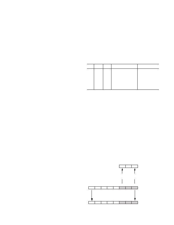
DB0
DB1
DB2
DB3
DB4
DB5
DB6
DB7
MSB
LSB
CONTROL BYTE
DB0
DB1
DB2
ADDRESS REGISTER
OVERTEMPERATURE
IF ANY BIT DB7 TO DB3 IS SET TO
A LOGIC 1 THEN THE FULL 8 BITS
OF THE CONTROL WORD ARE WRITTEN
TO THE OVERTEMPERATURE REGISTER
IF DB7 TO DB3 ARE LOGIC 0
THEN DB2 TO DB0 ARE WRITTEN
TO THE ADDRESS REGISTER
DB0
DB1
DB2
DB3
DB4
DB5
DB6
DB7
Figure 4. Address and Overtemperature Register Selection
相关PDF资料 |
PDF描述 |
|---|---|
| VI-BTF-CX-B1 | CONVERTER MOD DC/DC 72V 75W |
| ACM28DTMS | CONN EDGECARD 56POS R/A .156 SLD |
| EMM40DRMT-S288 | CONN EDGECARD 80POS .156 EXTEND |
| TCJY336M016R0070 | CAP TANT 33UF 16V 20% 2917 |
| TAJB335K016H | CAP TANT 3.3UF 16V 10% 1210 |
相关代理商/技术参数 |
参数描述 |
|---|---|
| AD7819 | 制造商:AD 制造商全称:Analog Devices 功能描述:+2.7 V to +5.5 V, 200 kSPS 8-Bit Sampling ADC |
| AD7819YN | 制造商:Analog Devices 功能描述:ADC Single SAR 200ksps 8-bit Parallel 16-Pin PDIP 制造商:Analog Devices 功能描述:IC 8BIT ADC 7819 DIP16 |
| AD7819YNZ | 功能描述:IC ADC 8BIT SAMPLING PAR 16-DIP RoHS:是 类别:集成电路 (IC) >> 数据采集 - 模数转换器 系列:- 其它有关文件:TSA1204 View All Specifications 标准包装:1 系列:- 位数:12 采样率(每秒):20M 数据接口:并联 转换器数目:2 功率耗散(最大):155mW 电压电源:模拟和数字 工作温度:-40°C ~ 85°C 安装类型:表面贴装 封装/外壳:48-TQFP 供应商设备封装:48-TQFP(7x7) 包装:Digi-Reel® 输入数目和类型:4 个单端,单极;2 个差分,单极 产品目录页面:1156 (CN2011-ZH PDF) 其它名称:497-5435-6 |
| AD7819YR | 制造商:Analog Devices 功能描述:ADC Single SAR 200ksps 8-bit Parallel 16-Pin SOIC N 制造商:Rochester Electronics LLC 功能描述:8 BIT,SINGLE,PARALLEL ADC I.C. - Bulk 制造商:Analog Devices 功能描述:IC SEMICONDUTOR ((NS)) |
| AD7819YR-REEL | 制造商:Analog Devices 功能描述:ADC Single SAR 200ksps 8-bit Parallel 16-Pin SOIC N T/R 制造商:Analog Devices 功能描述:ADC SGL SAR 200KSPS 8BIT PARALLEL 16SOIC N - Tape and Reel |
发布紧急采购,3分钟左右您将得到回复。