- 您现在的位置:买卖IC网 > PDF目录19466 > AD7818ARZ-REEL7 (Analog Devices Inc)IC ADC 10BIT W/TEMP SENSOR 8SOIC PDF资料下载
参数资料
| 型号: | AD7818ARZ-REEL7 |
| 厂商: | Analog Devices Inc |
| 文件页数: | 11/20页 |
| 文件大小: | 279K |
| 描述: | IC ADC 10BIT W/TEMP SENSOR 8SOIC |
| 标准包装: | 1,000 |
| 功能: | 温度监控系统(传感器) |
| 传感器类型: | 内部 |
| 感应温度: | -55°C ~ 125°C |
| 精确度: | ±2°C |
| 拓扑: | ADC,多路复用器,寄存器库 |
| 输出类型: | MICROWIRE?,QSPI?,SPI? |
| 输出警报: | 是 |
| 输出风扇: | 是 |
| 电源电压: | 2.7 V ~ 5.5 V |
| 工作温度: | -40°C ~ 85°C |
| 安装类型: | 表面贴装 |
| 封装/外壳: | 8-SOIC(0.154",3.90mm 宽) |
| 供应商设备封装: | 8-SO |
| 包装: | 带卷 (TR) |
REV. C
AD7816/AD7817/AD7818
11
MSB
LSB
0
0
0
0
0
0
0
1
MINIMUM TEMPERATURE = 95
C
1
1
1
1
1
1
1
1
MAXIMUM TEMPERATURE = +152
C
OVERTEMPERATURE REGISTER (DEC) = T
ALARM
+ 103C
T
ALARM
RESOLUTION = 1/ LSB
OVERTEMPERATURE REGISTER
DB0
DB1
DB2
DB3
DB4
DB5
DB6
DB7
Figure 5. The Overtemperature Register (OTR)
CIRCUIT INFORMATION
The AD7817 and AD7818 are single- and four-channel, 9 祍
conversion time, 10-bit A/D converters with on-chip tempera-
ture sensor, reference, and serial interface logic functions on a
single chip. The AD7816 has no analog input channel and is
intended for temperature measurement only. The A/D converter
section consists of a conventional successive-approximation
converter based around a capacitor DAC. The AD7816,
AD7817, and AD7818 are capable of running on a 2.7 V to
5.5 V power supply and the AD7817 and AD7818 accept an
analog input range of 0 V to +V
REF
. The on-chip temperature
sensor allows an accurate measurement of the ambient device
temperature to be made. The working measurement range of
the temperature sensor is 55癈 to +125癈. The part requires a
2.5 V reference, which can be provided from the parts own
internal reference or from an external reference source. The
on-chip reference is selected by connecting the REF
IN
pin to
analog ground.
CONVERTER DETAILS
Conversion is initiated by pulsing the CONVST input. The
conversion clock for the part is internally generated so no exter-
nal clock is required except when reading from and writing to
the serial port. The on-chip track/hold goes from track-to-hold
mode and the conversion sequence is started on the falling edge
of the CONVST signal. At this point the BUSY signal goes high
and low again 9 祍 or 27 祍 later (depending on whether an
analog input or the temperature sensor is selected) to indicate
the end of the conversion process. This signal can be used by a
microcontroller to determine when the result of the conversion
should be read. The track/hold acquisition time of the AD7817
and AD7818 is 400 ns.
A temperature measurement is made by selecting the Channel 0
of the on-chip MUX and carrying out a conversion on this
channel. A conversion on Channel 0 takes 27 祍 to complete.
Temperature measurement is explained in the Temperature
Measurement section of this data sheet.
The on-chip reference is not available to the user, but REF
IN
can be overdriven by an external reference source (2.5 V only).
The effect of reference tolerances on temperature measurements
is discussed in the section titled Temperature Measurement
Error Due to Reference Error.
All unused analog inputs should be tied to a voltage within the
nominal analog input range to avoid noise pickup. For mini-
mum power consumption, the unused analog inputs should be
tied to AGND.
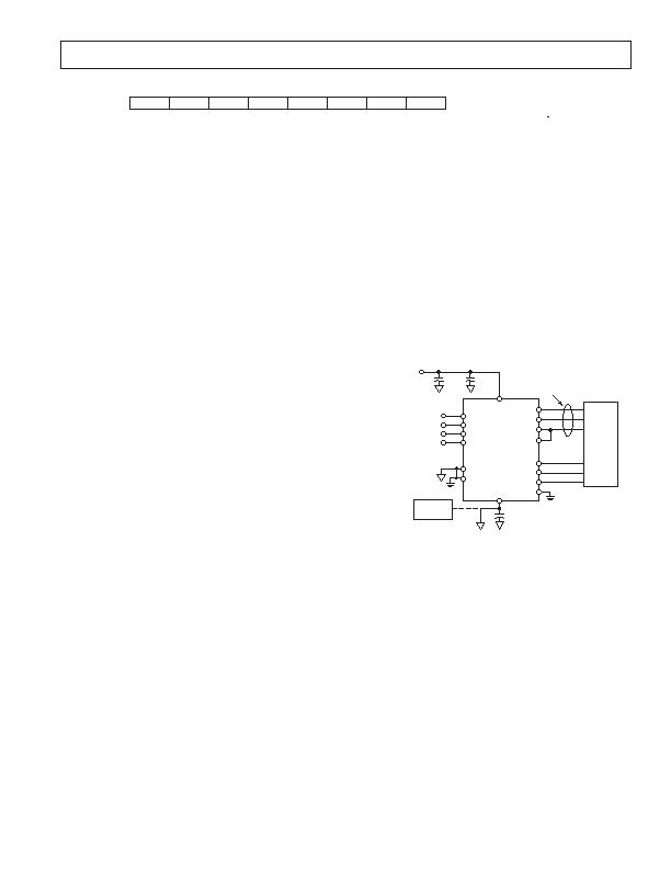
TYPICAL CONNECTION DIAGRAM
Figure 6 shows a typical connection diagram for the AD7817.
The AGND and DGND are connected together at the device
for good noise suppression. The BUSY line is used to interrupt
the microcontroller at the end of the conversion process and the
serial interface is implemented using three wiressee Serial
Interface section for more details. An external 2.5 V reference
can be connected at the REF
IN
pin. If an external reference is
used, a 10 礔 capacitor should be connected between REF
IN
and AGND. For applications where power consumption is of
concern, the automatic power-down at the end of a conversion
should be used to improve power performance. See Power vs.
Throughput section of this data sheet.
V
DD
AIN1
CONVST
AGND
DGND
REF
IN
SUPPLY
2.7V TO
5.5V
0.1F
10F
10F
EXTERNAL
REFERENCE
OPTIONAL
EXTERNAL
EFERENCE
AD780/
REF-192
0V TO 2.5V
INPUT
D
OUT
RD/WR
AIN2
AIN3
AIN4
D
IN
BUSY
OTI
C/P
SCLK
3-WIRE
SERIAL
INTERFACE
CS
AD7817
Figure 6. Typical Connection Diagram
ANALOG INPUTS
Analog Input
Figure 7 shows an equivalent circuit of the analog input struc-
ture of the AD7817 and AD7818. The two diodes D1 and D2
provide ESD protection for the analog inputs. Care must be
taken to ensure that the analog input signal never exceeds the
supply rails by more than 200 mV. This will cause these diodes
to become forward biased and start conducting current into the
substrate. The maximum current these diodes can conduct
without causing irreversible damage to the part is 20 mA. The
capacitor C2 in Figure 7 is typically about 4 pF and can mostly
be attributed to pin capacitance. The resistor R1 is a lumped
component made up of the on resistance of a multiplexer and a
switch. This resistor is typically about 1 k&. The capacitor C1 is
the ADC sampling capacitor and has a capacitance of 3 pF.
相关PDF资料 |
PDF描述 |
|---|---|
| VI-BTF-CX-B1 | CONVERTER MOD DC/DC 72V 75W |
| ACM28DTMS | CONN EDGECARD 56POS R/A .156 SLD |
| EMM40DRMT-S288 | CONN EDGECARD 80POS .156 EXTEND |
| TCJY336M016R0070 | CAP TANT 33UF 16V 20% 2917 |
| TAJB335K016H | CAP TANT 3.3UF 16V 10% 1210 |
相关代理商/技术参数 |
参数描述 |
|---|---|
| AD7819 | 制造商:AD 制造商全称:Analog Devices 功能描述:+2.7 V to +5.5 V, 200 kSPS 8-Bit Sampling ADC |
| AD7819YN | 制造商:Analog Devices 功能描述:ADC Single SAR 200ksps 8-bit Parallel 16-Pin PDIP 制造商:Analog Devices 功能描述:IC 8BIT ADC 7819 DIP16 |
| AD7819YNZ | 功能描述:IC ADC 8BIT SAMPLING PAR 16-DIP RoHS:是 类别:集成电路 (IC) >> 数据采集 - 模数转换器 系列:- 其它有关文件:TSA1204 View All Specifications 标准包装:1 系列:- 位数:12 采样率(每秒):20M 数据接口:并联 转换器数目:2 功率耗散(最大):155mW 电压电源:模拟和数字 工作温度:-40°C ~ 85°C 安装类型:表面贴装 封装/外壳:48-TQFP 供应商设备封装:48-TQFP(7x7) 包装:Digi-Reel® 输入数目和类型:4 个单端,单极;2 个差分,单极 产品目录页面:1156 (CN2011-ZH PDF) 其它名称:497-5435-6 |
| AD7819YR | 制造商:Analog Devices 功能描述:ADC Single SAR 200ksps 8-bit Parallel 16-Pin SOIC N 制造商:Rochester Electronics LLC 功能描述:8 BIT,SINGLE,PARALLEL ADC I.C. - Bulk 制造商:Analog Devices 功能描述:IC SEMICONDUTOR ((NS)) |
| AD7819YR-REEL | 制造商:Analog Devices 功能描述:ADC Single SAR 200ksps 8-bit Parallel 16-Pin SOIC N T/R 制造商:Analog Devices 功能描述:ADC SGL SAR 200KSPS 8BIT PARALLEL 16SOIC N - Tape and Reel |
发布紧急采购,3分钟左右您将得到回复。