- 您现在的位置:买卖IC网 > PDF目录10796 > AD7834AR-REEL (Analog Devices Inc)IC DAC 14BIT QUAD SRL 28-SOIC PDF资料下载
参数资料
| 型号: | AD7834AR-REEL |
| 厂商: | Analog Devices Inc |
| 文件页数: | 17/28页 |
| 文件大小: | 0K |
| 描述: | IC DAC 14BIT QUAD SRL 28-SOIC |
| 产品培训模块: | Data Converter Fundamentals DAC Architectures |
| 产品变化通告: | Product Discontinuance 27/Oct/2011 |
| 标准包装: | 1,000 |
| 设置时间: | 10µs |
| 位数: | 14 |
| 数据接口: | 串行 |
| 转换器数目: | 4 |
| 电压电源: | 模拟和数字,双 ± |
| 功率耗散(最大): | 465mW |
| 工作温度: | -40°C ~ 85°C |
| 安装类型: | 表面贴装 |
| 封装/外壳: | 28-SOIC(0.295",7.50mm 宽) |
| 供应商设备封装: | 28-SOIC W |
| 包装: | 带卷 (TR) |
| 输出数目和类型: | 4 电压,单极;4 电压,双极 |
| 采样率(每秒): | 100k |
第1页第2页第3页第4页第5页第6页第7页第8页第9页第10页第11页第12页第13页第14页第15页第16页当前第17页第18页第19页第20页第21页第22页第23页第24页第25页第26页第27页第28页
AD7834/AD7835
Rev. D | Page 24 of 28
4
6
8
13
7
3
1
15
14
9
16
2
10 11 12
1F
+15V –15V
0.1F
AD588
4
6
8
13
7
3
1
15
14
16
2
10
11
12
1F
+15V –15V
AD588
9
DUT
GND
TO TESTER
WINDOW
COMPARATOR
–15V
+15V
VREF(+)A
VREF(–)A
DSG A
VREF(+)B
VREF(–)B
AD78351
VOUT1
VOUT2
VOUT3
VOUT4
DSG B
AGND
DUT
GND
DUT
GND
VDUT
VOFFSET
PIN
DRIVER
01006
-035
1ADDITIONAL PINS OMITTED FOR CLARITY
If the AD7834/AD7835 are the only devices requiring an AGND
to DGND connection, then the ground planes should be connected
at the AGND and DGND pins of the AD7834/ AD7835. If the
AD7834/AD7835 are in a system where multiple devices require
an AGND to DGND connection, the connection can still be made
at one point only, a star ground point, which can be established as
close as possible to the AD7834/AD7835.
Digital lines running under the device must be avoided because
they couple noise onto the die. The analog ground plane can run
under the AD7834/AD7835 to avoid noise coupling. The power
supply lines of the AD7834/AD7835 can use as large a trace as
possible to provide low impedance paths and reduce the effects of
glitches on the power supply line. Fast switching signals, such as
clocks, should be shielded with digital ground to avoid radiating
noise to other parts of the board. These signals should never be
run near the analog inputs. Avoid crossover of digital and analog
signals. Traces on opposite sides of the board should run at right
angles to each other. This reduces the effects of feedthrough
through the board. A microstrip method is best but not always
possible with a double-sided board. With this method, the
component side of the board is dedicated to ground plane while
signal traces are placed on the solder side.
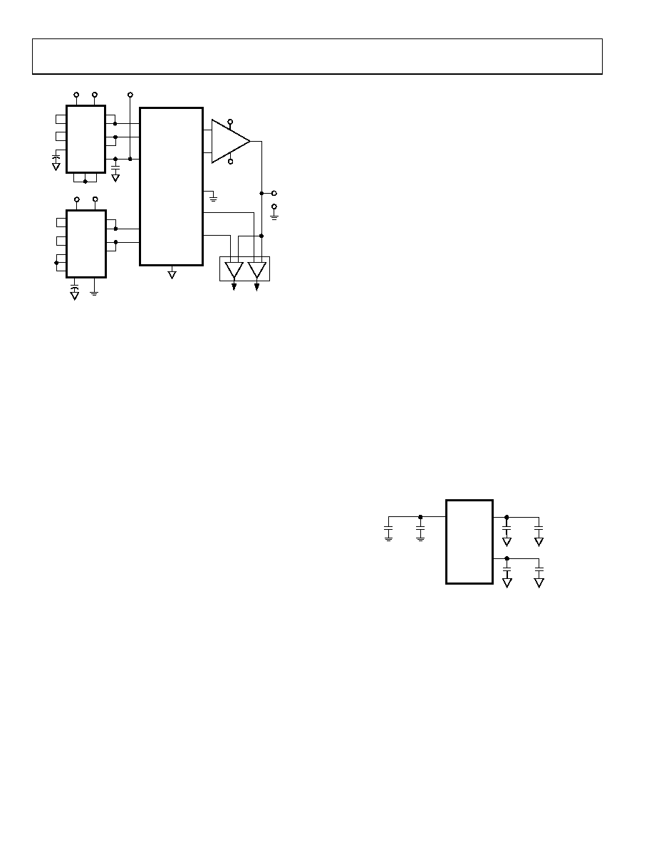
Figure 35. ATE Application
The other AD588 provides a reference voltage for DAC 3 and
DAC 4. These provide the reference voltages for the window
nected to DUT GND. This causes VREF(+)B and VREF()B to be
referenced to DUT GND. As DAC 3 and DAC 4 input codes vary
from 000 . . . 000 to 111 . . . 111, VOUT3 and VOUT4 vary from 5 V
to +5 V with respect to DUT GND. DUT GND is also connected
to DSGB. When the AD7835 is cleared, VOUT3 and VOUT4 are
cleared to 0 V with respect to DUT GND.
The AD7834/AD7835 must have ample supply bypassing located
as close as possible to the package, ideally right up against the
device. Figure 36 shows the recommended capacitor values of
10 μF in parallel with 0.1 μF on each of the supplies. The 10 μF
capacitors are the tantalum bead type. The 0.1 μF capacitor can
have low effective series resistance (ESR) and effective series
inductance (ESI), such as the common ceramic types, which
provide a low impedance path to ground at high frequencies to
handle transient currents due to internal logic switching.
Care must be taken to ensure that the maximum and minimum
voltage specifications for the AD7835 reference voltages are
followed as shown in Figure 35.
10
μF
0.1
μF
1ADDITIONAL PINS OMITTED FOR CLARITY
10
μF
0.1
μF
10
μF
0.1
μF
AD7834/
AD78351
VDD
VCC
VSS
AGND
DGND
01006-036
POWER SUPPLY BYPASSING AND GROUNDING
In any circuit where accuracy is important, careful considera-
tion of the power supply and ground return layout helps to
ensure the rated performance. The printed circuit boards on
which the AD7834/AD7835 are mounted should be designed so
the analog and digital sections are separated and confined to
certain areas of the boards. This facilitates the use of ground
planes that can be easily separated. A minimum etch technique
is generally best for ground planes because it gives the best
shielding. Digital and analog ground planes should be joined at
only one place.
Figure 36. Power Supply Decoupling
相关PDF资料 |
PDF描述 |
|---|---|
| LT319AN#PBF | IC COMPARATOR DUAL 14-DIP |
| LTC1685IS8#PBF | IC TXRX RS485 PREC DELAY 8-SOIC |
| AD7628KP | IC DAC 8BIT DUAL W/BUFF 20-PLCC |
| LTC1042CN8#PBF | IC CMOS COMPARATOR WINDOW 8DIP |
| AD7549AQ | IC DAC 12BIT DUAL LC2MOS 20-CDIP |
相关代理商/技术参数 |
参数描述 |
|---|---|
| AD7834ARZ | 功能描述:IC DAC 14BIT QUAD SRL 28-SOIC RoHS:是 类别:集成电路 (IC) >> 数据采集 - 数模转换器 系列:- 标准包装:1 系列:- 设置时间:4.5µs 位数:12 数据接口:串行,SPI? 转换器数目:1 电压电源:单电源 功率耗散(最大):- 工作温度:-40°C ~ 125°C 安装类型:表面贴装 封装/外壳:8-SOIC(0.154",3.90mm 宽) 供应商设备封装:8-SOICN 包装:剪切带 (CT) 输出数目和类型:1 电压,单极;1 电压,双极 采样率(每秒):* 其它名称:MCP4921T-E/SNCTMCP4921T-E/SNRCTMCP4921T-E/SNRCT-ND |
| AD7834ARZ-REEL | 功能描述:IC DAC 14BIT QUAD SERIAL 28SOIC RoHS:是 类别:集成电路 (IC) >> 数据采集 - 数模转换器 系列:- 产品培训模块:Data Converter Fundamentals DAC Architectures 标准包装:750 系列:- 设置时间:7µs 位数:16 数据接口:并联 转换器数目:1 电压电源:双 ± 功率耗散(最大):100mW 工作温度:0°C ~ 70°C 安装类型:表面贴装 封装/外壳:28-LCC(J 形引线) 供应商设备封装:28-PLCC(11.51x11.51) 包装:带卷 (TR) 输出数目和类型:1 电压,单极;1 电压,双极 采样率(每秒):143k |
| AD7834BN | 制造商:Analog Devices 功能描述:DAC 4-CH R-2R 14-bit 28-Pin PDIP W Tube 制造商:Rochester Electronics LLC 功能描述:QUAD 14 BIT SERIAL DAC IC - Bulk |
| AD7834BNZ | 制造商:Analog Devices 功能描述:DAC 4-CH R-2R 14-bit 28-Pin PDIP W Tube |
| AD7834BR | 功能描述:IC DAC 14BIT QUAD SRL 28-SOIC RoHS:否 类别:集成电路 (IC) >> 数据采集 - 数模转换器 系列:- 产品培训模块:Lead (SnPb) Finish for COTS Obsolescence Mitigation Program 标准包装:1,000 系列:- 设置时间:1µs 位数:8 数据接口:串行 转换器数目:8 电压电源:双 ± 功率耗散(最大):941mW 工作温度:0°C ~ 70°C 安装类型:表面贴装 封装/外壳:24-SOIC(0.295",7.50mm 宽) 供应商设备封装:24-SOIC W 包装:带卷 (TR) 输出数目和类型:8 电压,单极 采样率(每秒):* |
发布紧急采购,3分钟左右您将得到回复。