- 您现在的位置:买卖IC网 > PDF目录10796 > AD7834AR-REEL (Analog Devices Inc)IC DAC 14BIT QUAD SRL 28-SOIC PDF资料下载
参数资料
| 型号: | AD7834AR-REEL |
| 厂商: | Analog Devices Inc |
| 文件页数: | 9/28页 |
| 文件大小: | 0K |
| 描述: | IC DAC 14BIT QUAD SRL 28-SOIC |
| 产品培训模块: | Data Converter Fundamentals DAC Architectures |
| 产品变化通告: | Product Discontinuance 27/Oct/2011 |
| 标准包装: | 1,000 |
| 设置时间: | 10µs |
| 位数: | 14 |
| 数据接口: | 串行 |
| 转换器数目: | 4 |
| 电压电源: | 模拟和数字,双 ± |
| 功率耗散(最大): | 465mW |
| 工作温度: | -40°C ~ 85°C |
| 安装类型: | 表面贴装 |
| 封装/外壳: | 28-SOIC(0.295",7.50mm 宽) |
| 供应商设备封装: | 28-SOIC W |
| 包装: | 带卷 (TR) |
| 输出数目和类型: | 4 电压,单极;4 电压,双极 |
| 采样率(每秒): | 100k |
第1页第2页第3页第4页第5页第6页第7页第8页当前第9页第10页第11页第12页第13页第14页第15页第16页第17页第18页第19页第20页第21页第22页第23页第24页第25页第26页第27页第28页
AD7834/AD7835
Rev. D | Page 17 of 28
CONTROLLED POWER-ON OF THE OUTPUT STAGE
DAC
G1
G3
VOUT
R
G6
G4
G5
G2
DSG
01006-023
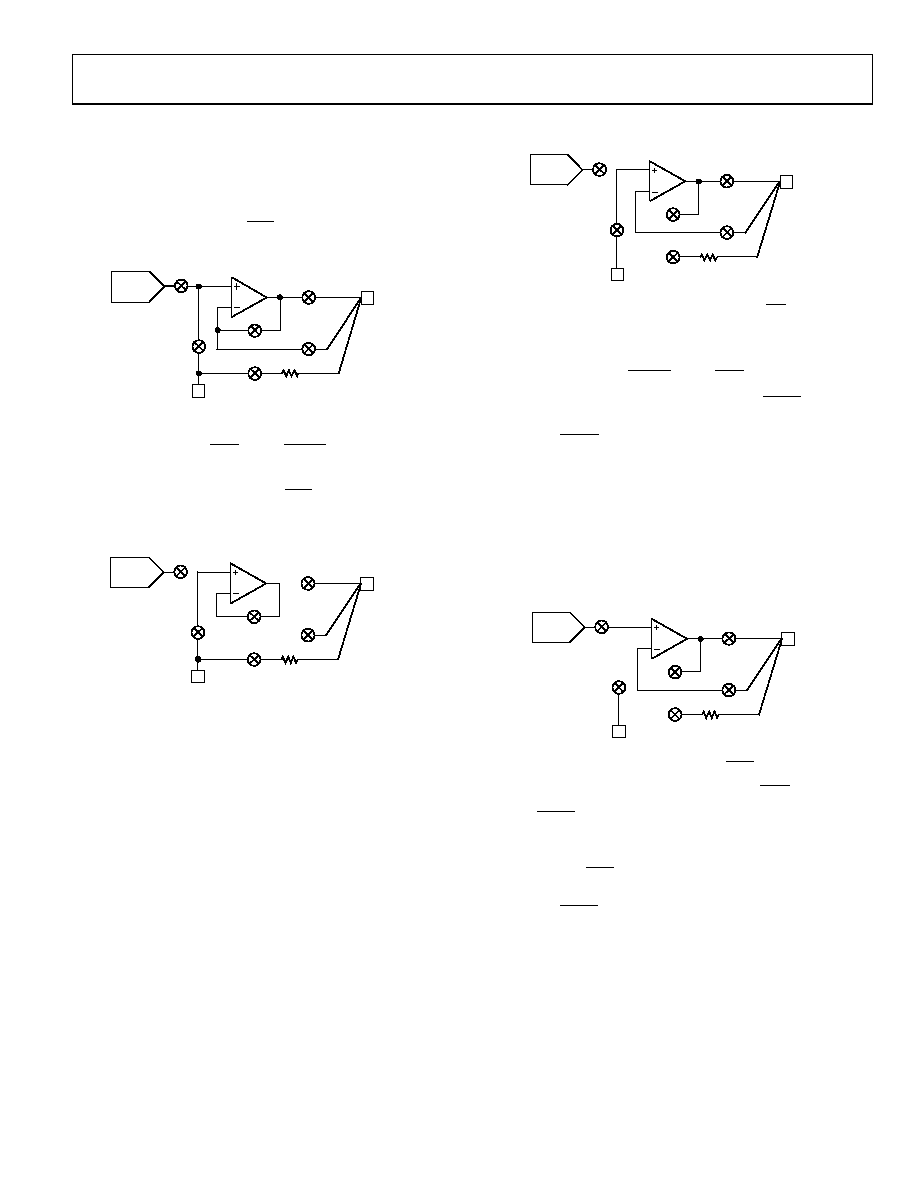
A block diagram of the output stage of the AD7834/AD7835 is
shown in Figure 21. It is capable of driving a load of 10 kΩ in
parallel with 200 pF. G1 to G6 are transmission gates used to
control the power-on voltage present at VOUT. G1 and G2 are also
used in conjunction with the CLR input to set VOUT to the user-
defined voltage present at the DSG pin.
DAC
G1
G3
VOUT
R
G6
G4
G5
G2
DSG
01006-021
Figure 23. Output Stage with VDD > 10 V and CLR Low
VOUT is disconnected from the DSG pin by the opening of G5
but tracks the voltage present at DSG via the unity gain buffer.
Figure 21. Block Diagram of AD7834/AD7835 Output Stage
POWER-ON WITH CLR LOW, LDAC HIGH
The output stage of the AD7834/AD7835 is designed to allow
output stability during power-on. If CLR is kept low during
power-on, and power is applied to the part, G1, G4, and G6 are
DAC
G1
G3
VOUT
R
G6
G4
G5
G2
DSG
01006-022
Figure 22. Output Stage with VDD < 10 V
VOUT is kept within a few hundred millivolts of DSG via G5
and R. R is a thin-film resistor between DSG and VOUT. The
output amplifier is connected as a unity gain buffer via G3, and
the DSG voltage is applied to the buffer input via G2. The
amplifier output is thus at the same voltage as the DSG pin. The
output stage remains configured as in Figure 22 until the
voltage at VDD and VSS reaches approximately ±10 V. At this
point, the output amplifier has enough headroom to handle
signals at its input and has also had time to settle. The internal
power-on circuitry opens G3 and G5 and closes G4 and G6 (see
Figure 23). As a result, the output amplifier is connected in
unity gain mode via G4 and G6. The DSG voltage is still applied
to the noninverting input via G2. This voltage appears at VOUT.
POWER-ON WITH LDAC LOW, CLR HIGH
LDAC
In many applications of the AD7834/AD7835,
is kept
continuously low, updating the DAC after each valid data
transfer. If LDAC is low when power is applied, G1 is closed and
G2 is open, connecting the output of the DAC to the input of the
output amplifier. G3 and G5 are closed and G4 and G6 are open,
connecting the amplifier as a unity gain buffer, as before. VOUT is
connected to DSG via G5 and R (a thin-film resistance between
DSG and VOUT) until VDD and VSS reach approximately ±10 V.
Then, the internal power-on circuitry opens G3 and G5 and
this point, VOUT is at the same voltage as the DAC output.
DAC
G1
G3
VOUT
R
G6
G4
G5
G2
DSG
01006-024
LDAC
Figure 24. Output Stage with
Low
LOADING THE DAC AND USING THE CLR INPUT
LDAC
When
The voltage at VOUT now follows the voltage present at the out-
put of the DAC. The output stage remains connected in this
manner until a CLR signal is applied. Then, the situation reverts
DSG until LDAC goes low. This reconnects the DAC output to
the unity gain buffer.
相关PDF资料 |
PDF描述 |
|---|---|
| LT319AN#PBF | IC COMPARATOR DUAL 14-DIP |
| LTC1685IS8#PBF | IC TXRX RS485 PREC DELAY 8-SOIC |
| AD7628KP | IC DAC 8BIT DUAL W/BUFF 20-PLCC |
| LTC1042CN8#PBF | IC CMOS COMPARATOR WINDOW 8DIP |
| AD7549AQ | IC DAC 12BIT DUAL LC2MOS 20-CDIP |
相关代理商/技术参数 |
参数描述 |
|---|---|
| AD7834ARZ | 功能描述:IC DAC 14BIT QUAD SRL 28-SOIC RoHS:是 类别:集成电路 (IC) >> 数据采集 - 数模转换器 系列:- 标准包装:1 系列:- 设置时间:4.5µs 位数:12 数据接口:串行,SPI? 转换器数目:1 电压电源:单电源 功率耗散(最大):- 工作温度:-40°C ~ 125°C 安装类型:表面贴装 封装/外壳:8-SOIC(0.154",3.90mm 宽) 供应商设备封装:8-SOICN 包装:剪切带 (CT) 输出数目和类型:1 电压,单极;1 电压,双极 采样率(每秒):* 其它名称:MCP4921T-E/SNCTMCP4921T-E/SNRCTMCP4921T-E/SNRCT-ND |
| AD7834ARZ-REEL | 功能描述:IC DAC 14BIT QUAD SERIAL 28SOIC RoHS:是 类别:集成电路 (IC) >> 数据采集 - 数模转换器 系列:- 产品培训模块:Data Converter Fundamentals DAC Architectures 标准包装:750 系列:- 设置时间:7µs 位数:16 数据接口:并联 转换器数目:1 电压电源:双 ± 功率耗散(最大):100mW 工作温度:0°C ~ 70°C 安装类型:表面贴装 封装/外壳:28-LCC(J 形引线) 供应商设备封装:28-PLCC(11.51x11.51) 包装:带卷 (TR) 输出数目和类型:1 电压,单极;1 电压,双极 采样率(每秒):143k |
| AD7834BN | 制造商:Analog Devices 功能描述:DAC 4-CH R-2R 14-bit 28-Pin PDIP W Tube 制造商:Rochester Electronics LLC 功能描述:QUAD 14 BIT SERIAL DAC IC - Bulk |
| AD7834BNZ | 制造商:Analog Devices 功能描述:DAC 4-CH R-2R 14-bit 28-Pin PDIP W Tube |
| AD7834BR | 功能描述:IC DAC 14BIT QUAD SRL 28-SOIC RoHS:否 类别:集成电路 (IC) >> 数据采集 - 数模转换器 系列:- 产品培训模块:Lead (SnPb) Finish for COTS Obsolescence Mitigation Program 标准包装:1,000 系列:- 设置时间:1µs 位数:8 数据接口:串行 转换器数目:8 电压电源:双 ± 功率耗散(最大):941mW 工作温度:0°C ~ 70°C 安装类型:表面贴装 封装/外壳:24-SOIC(0.295",7.50mm 宽) 供应商设备封装:24-SOIC W 包装:带卷 (TR) 输出数目和类型:8 电压,单极 采样率(每秒):* |
发布紧急采购,3分钟左右您将得到回复。