参数资料
| 型号: | AD7840KNZ |
| 厂商: | Analog Devices Inc |
| 文件页数: | 11/16页 |
| 文件大小: | 0K |
| 描述: | IC DAC 14BIT LC2MOS VOUT 24-DIP |
| 产品培训模块: | Data Converter Fundamentals DAC Architectures |
| 标准包装: | 15 |
| 设置时间: | 2.5µs |
| 位数: | 14 |
| 数据接口: | 串行,并联 |
| 转换器数目: | 1 |
| 电压电源: | 双 ± |
| 功率耗散(最大): | 100mW |
| 工作温度: | 0°C ~ 70°C |
| 安装类型: | 通孔 |
| 封装/外壳: | 24-DIP(0.300",7.62mm) |
| 供应商设备封装: | 24-PDIP |
| 包装: | 管件 |
| 输出数目和类型: | 1 电压,双极 |
| 采样率(每秒): | 400k |
AD7840
REV. B
–4–
PIN FUNCTION DESCRIPTION
DIP
Pin
No.
Mnemonic
Function
1
CS
/SERIAL
Chip Select/Serial Input. When driven with normal logic levels, it is an active low logic input which is used
in conjunction with WR to load parallel data to the input latch. For applications where CS is perma-
nently low, an R, C is required for correct power-up (see LDAC input). If this input is tied to VSS, it de-
fines the AD7840 for serial mode operation.
2
WR/SYNC
Write/Frame Synchronization Input. In the parallel data mode, it is used in conjunction with CS to load
parallel data. In the serial mode of operation, this pin functions as a Frame Synchronization pulse with se-
rial data expected after the falling edge of this signal.
3
D13/SDATA
Data Bit 13(MSB)/Serial Data. When parallel data is selected, this pin is the D13 input. In serial mode,
SDATA is the serial data input which is used in conjunction with SYNC and SCLK to transfer serial data
to the AD7840 input latch.
4
D12/SCLK
Data Bit 12/Serial Clock. When parallel data is selected, this pin is the D12 input. In the serial mode, it is
the serial clock input. Serial data bits are latched on the falling edge of SCLK when SYNC is low.
5
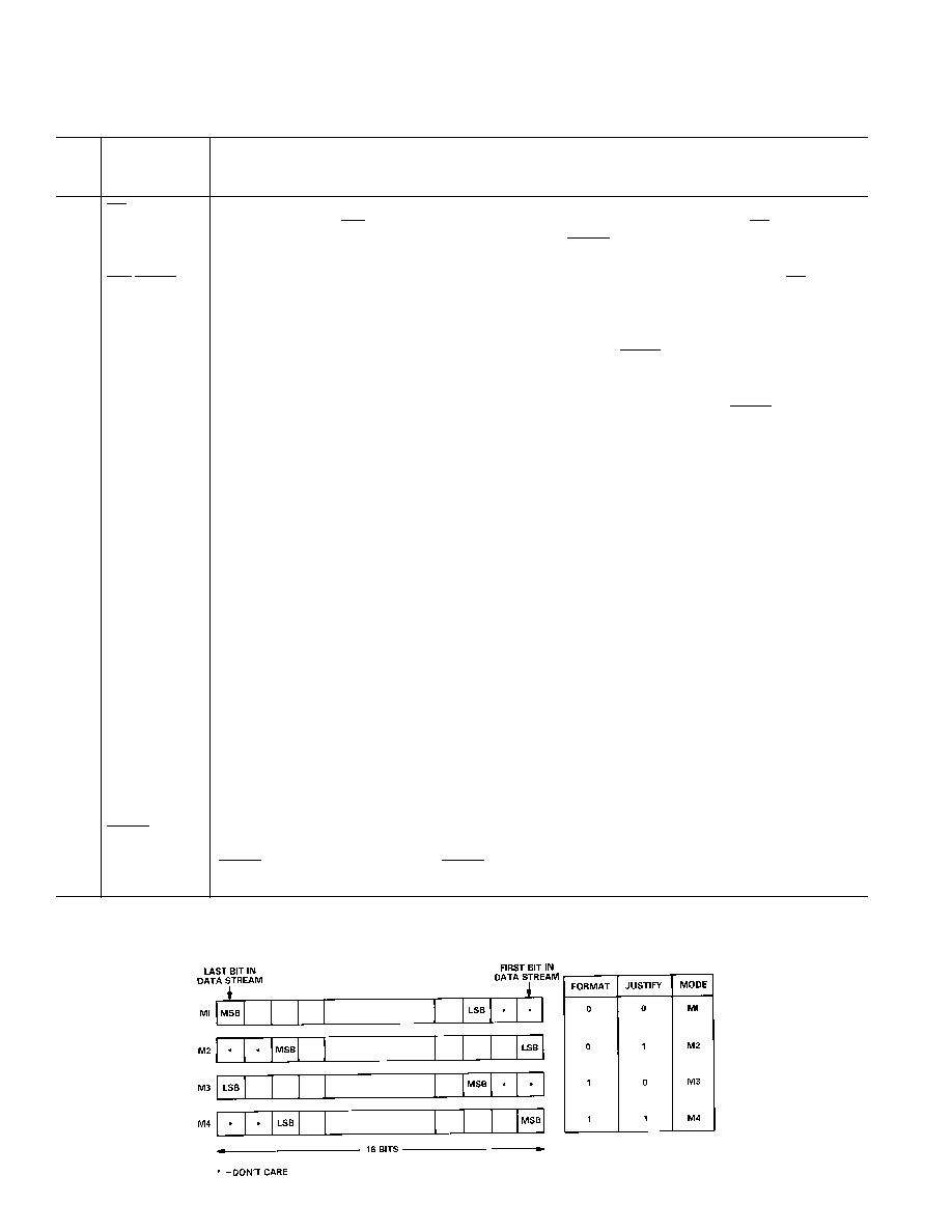
D11/FORMAT
Data Bit 11/Data Format. When parallel data is selected, this pin is the D11 input. In serial mode, a Logic
1 on this input indicates that the MSB is the first valid bit in the serial data stream. A Logic 0 indicates
that the LSB is the first valid bit (see Table I).
6
D10/JUSTIFY
Data Bit 10/Data Justification. When parallel data is selected, this pin is the D10 input. In serial mode,
this input controls the serial data justification (see Table I).
7–11
D9–D5
Data Bit 9 to Data Bit 5. Parallel data inputs.
12
DGND
Digital Ground. Ground reference for digital circuitry.
13–16
D4–D1
Data Bit 4 to Data Bit 1. Parallel data inputs.
17
D0
Data Bit 0 (LSB). Parallel data input.
18
VDD
Positive Supply, +5 V
± 5%.
19
AGND
Analog Ground. Ground reference for DAC, reference and output buffer amplifier.
20
VOUT
Analog Output Voltage. This is the buffer amplifier output voltage. Bipolar output range (
±3 V with REF
IN = +3 V).
21
VSS
Negative Supply Voltage, –5 V
± 5%.
22
REF OUT
Voltage Reference Output. The internal 3 V analog reference is provided at this pin. To operate the
AD7840 with internal reference, REF OUT should be connected to REF IN. The external load capability
of the reference is 500
A.
23
REF IN
Voltage Reference Input. The reference voltage for the DAC is applied to this pin. It is internally buffered
before being applied to the DAC. The nominal reference voltage for correct operation of the AD7840 is
3 V.
24
LDAC
Load DAC. Logic Input. A new word is loaded into the DAC latch from the input latch on the falling
edge of this signal (see Interface Logic Information section). The AD7840 should be powered-up with
LDAC
high. For applications where LDAC is permanently low, an R, C is required for correct power-up
(see Figure 19).
Table I. Serial Data Modes
相关PDF资料 |
PDF描述 |
|---|---|
| AD7248AAP | IC DAC 12BIT W/REF 28-PLCC |
| AD5570WRSZ-REEL | IC DAC 16BIT SERIAL IN 16SSOP |
| AD5544ARSZ-REEL7 | IC DAC 16BIT QUAD SRL 28SSOP |
| AD7228ACPZ-REEL | IC DAC 8BIT OCTAL W/AMP 28-PLCC |
| AD7228ACRZ-REEL | IC DAC 8BIT OCTAL W/AMP 24SOIC |
相关代理商/技术参数 |
参数描述 |
|---|---|
| AD7840KP | 功能描述:IC DAC 14BIT LOW PWR 5V 28-PLCC RoHS:否 类别:集成电路 (IC) >> 数据采集 - 数模转换器 系列:- 产品培训模块:Data Converter Fundamentals DAC Architectures 标准包装:750 系列:- 设置时间:7µs 位数:16 数据接口:并联 转换器数目:1 电压电源:双 ± 功率耗散(最大):100mW 工作温度:0°C ~ 70°C 安装类型:表面贴装 封装/外壳:28-LCC(J 形引线) 供应商设备封装:28-PLCC(11.51x11.51) 包装:带卷 (TR) 输出数目和类型:1 电压,单极;1 电压,双极 采样率(每秒):143k |
| AD7840KP-REEL | 功能描述:14 Bit Digital to Analog Converter 1 28-PLCC (11.51x11.51) 制造商:analog devices inc. 系列:- 包装:带卷(TR) 零件状态:上次购买时间 位数:14 数模转换器数:1 建立时间:4μs 输出类型:Voltage - Buffered 差分输出:无 数据接口:并联,串行 参考类型:外部, 内部 电压 - 电源,模拟:±5V 电压 - 电源,数字:- INL/DNL(LSB):±1(最大),±0.9(最大) 架构:R-2R 工作温度:0°C ~ 70°C 封装/外壳:28-LCC(J 形引线) 供应商器件封装:28-PLCC(11.51x11.51) 标准包装:1 |
| AD7840KPZ | 功能描述:IC DAC 14BIT LOW PWR 5V 28-PLCC RoHS:是 类别:集成电路 (IC) >> 数据采集 - 数模转换器 系列:- 产品培训模块:Data Converter Fundamentals DAC Architectures 标准包装:750 系列:- 设置时间:7µs 位数:16 数据接口:并联 转换器数目:1 电压电源:双 ± 功率耗散(最大):100mW 工作温度:0°C ~ 70°C 安装类型:表面贴装 封装/外壳:28-LCC(J 形引线) 供应商设备封装:28-PLCC(11.51x11.51) 包装:带卷 (TR) 输出数目和类型:1 电压,单极;1 电压,双极 采样率(每秒):143k |
| AD7840KPZ-RL | 功能描述:14 Bit Digital to Analog Converter 1 28-PLCC (11.51x11.51) 制造商:analog devices inc. 系列:- 包装:带卷(TR) 零件状态:在售 位数:14 数模转换器数:1 建立时间:4μs 输出类型:Voltage - Buffered 差分输出:无 数据接口:并联,串行 参考类型:外部, 内部 电压 - 电源,模拟:±5V 电压 - 电源,数字:- INL/DNL(LSB):±1(最大),±0.9(最大) 架构:R-2R 工作温度:0°C ~ 70°C 封装/外壳:28-LCC(J 形引线) 供应商器件封装:28-PLCC(11.51x11.51) 标准包装:1 |
| AD7840LN | 制造商:未知厂家 制造商全称:未知厂家 功能描述:14-Bit Digital-to-Analog Converter |
发布紧急采购,3分钟左右您将得到回复。