参数资料
| 型号: | AD7840KNZ |
| 厂商: | Analog Devices Inc |
| 文件页数: | 13/16页 |
| 文件大小: | 0K |
| 描述: | IC DAC 14BIT LC2MOS VOUT 24-DIP |
| 产品培训模块: | Data Converter Fundamentals DAC Architectures |
| 标准包装: | 15 |
| 设置时间: | 2.5µs |
| 位数: | 14 |
| 数据接口: | 串行,并联 |
| 转换器数目: | 1 |
| 电压电源: | 双 ± |
| 功率耗散(最大): | 100mW |
| 工作温度: | 0°C ~ 70°C |
| 安装类型: | 通孔 |
| 封装/外壳: | 24-DIP(0.300",7.62mm) |
| 供应商设备封装: | 24-PDIP |
| 包装: | 管件 |
| 输出数目和类型: | 1 电压,双极 |
| 采样率(每秒): | 400k |
AD7840
REV. B
–6–
OP AMP SECTION
The output from the voltage mode DAC is buffered by a
noninverting amplifier. Internal scaling resistors on the AD7840
configure an output voltage range of
±3 V for an input reference
voltage of +3 V. The arrangement of these resistors around the
output op amp is as shown in Figure 1. The buffer amplifier is
capable of developing
±3 V across a 2 k and 100 pF load to
ground and can produce 6 V peak-to-peak sine wave signals to a
frequency of 20 kHz. The output is updated on the falling edge
of the LDAC input. The amplifier settles to within 1/2 LSB of
its final value in typically less than 2.5
s.
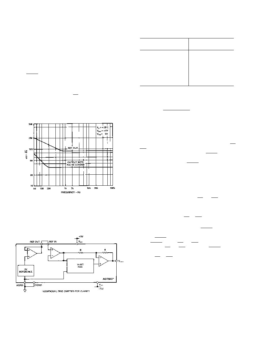
The small signal (200 mV p-p) bandwidth of the output buffer
amplifier is typically 1 MHz. The output noise from the ampli-
fier is low with a figure of 30 nV/
√Hz at a frequency of 1 kHz.
The broadband noise from the amplifier exhibits a typical peak-
to-peak figure of 150
V for a 1 MHz output bandwidth. Figure
4 shows a typical plot of noise spectral density versus frequency
for the output buffer amplifier and for the on-chip reference.
Figure 4. Noise Spectral Density vs. Frequency
TRANSFER FUNCTION
The basic circuit configuration for the AD7840 is shown in Fig-
ure 5. Table II shows the ideal input code to output voltage re-
lationship for this configuration. Input coding to the DAC is 2s
complement with 1 LSB = FS/16,384 = 6 V/16,384 = 366
V.
Figure 5. AD7840 Basic Connection Diagram
Table II. Ideal Input/Output Code Table
DAC Latch Contents
MSB
LSB
Analog Output, VOUT*
0 1 1 1 1 1 1 1 1 1 1 1 1 1
+2.999634 V
0 1 1 1 1 1 1 1 1 1 1 1 1 0
+2.999268 V
0 0 0 0 0 0 0 0 0 0 0 0 0 1
+0.000366 V
0 0 0 0 0 0 0 0 0 0 0 0 0 0
0 V
1 1 1 1 1 1 1 1 1 1 1 1 1 1
–0.000366 V
1 0 0 0 0 0 0 0 0 0 0 0 0 1
–2.999634 V
1 0 0 0 0 0 0 0 0 0 0 0 0 0
–3 V
*Assuming REF IN = +3 V.
The output voltage can be expressed in terms of the input code,
N, using the following expression:
V
OUT =
2
× N × REFIN
16384
8192 ≤ N ≤+8191
INTERFACE LOGIC INFORMATION
The AD7840 contains two 14-bit latches, an input latch and a
DAC latch. Data can be loaded to the input latch in one of two
basic interface formats. The first is a parallel 14-bit wide data
word; the second is a serial interface where 16 bits of data are
serially clocked into the input latch. In the parallel mode, CS
and WR control the loading of data. When the serial data format
is selected, data is loaded using the SCLK, SYNC and SDATA
serial inputs. Data is transferred from the input latch to the
DAC latch under control of the LDAC signal. Only the data in
the DAC latch determines the analog output of the AD7840.
Parallel Data Format
Table III shows the truth table for AD7840 parallel mode op-
eration. The AD7840 normally operates with a parallel input
data format. In this case, all 14 bits of data (appearing on data
inputs D13 (MSB) through D0 (LSB)) are loaded to the
AD7840 input latch at the same time. CS and WR control the
loading of this data. These control signals are level-triggered;
therefore, the input latch can be made transparent by holding
both signals at a logic low level. Input data is latched into the in-
put latch on the rising edge of CS or WR.
The DAC latch is also level triggered. The DAC output is nor-
mally updated on the falling edge of the LDAC signal. However,
both latches cannot become transparent at the same time.
Therefore, if LDAC is hardwired low, the part operates as fol-
lows; with LDAC low and CS and WR high, the DAC latch is
transparent. When CS and WR go low (with LDAC still low),
the input latch becomes transparent but the DAC latch is dis-
abled. When CS or WR return high, the input latch is locked
out and the DAC latch becomes transparent again and the DAC
output is updated. The write cycle timing diagram for parallel
data is shown in Figure 6. Figure 7 shows the simplified parallel
input control logic for the AD7840.
相关PDF资料 |
PDF描述 |
|---|---|
| AD7248AAP | IC DAC 12BIT W/REF 28-PLCC |
| AD5570WRSZ-REEL | IC DAC 16BIT SERIAL IN 16SSOP |
| AD5544ARSZ-REEL7 | IC DAC 16BIT QUAD SRL 28SSOP |
| AD7228ACPZ-REEL | IC DAC 8BIT OCTAL W/AMP 28-PLCC |
| AD7228ACRZ-REEL | IC DAC 8BIT OCTAL W/AMP 24SOIC |
相关代理商/技术参数 |
参数描述 |
|---|---|
| AD7840KP | 功能描述:IC DAC 14BIT LOW PWR 5V 28-PLCC RoHS:否 类别:集成电路 (IC) >> 数据采集 - 数模转换器 系列:- 产品培训模块:Data Converter Fundamentals DAC Architectures 标准包装:750 系列:- 设置时间:7µs 位数:16 数据接口:并联 转换器数目:1 电压电源:双 ± 功率耗散(最大):100mW 工作温度:0°C ~ 70°C 安装类型:表面贴装 封装/外壳:28-LCC(J 形引线) 供应商设备封装:28-PLCC(11.51x11.51) 包装:带卷 (TR) 输出数目和类型:1 电压,单极;1 电压,双极 采样率(每秒):143k |
| AD7840KP-REEL | 功能描述:14 Bit Digital to Analog Converter 1 28-PLCC (11.51x11.51) 制造商:analog devices inc. 系列:- 包装:带卷(TR) 零件状态:上次购买时间 位数:14 数模转换器数:1 建立时间:4μs 输出类型:Voltage - Buffered 差分输出:无 数据接口:并联,串行 参考类型:外部, 内部 电压 - 电源,模拟:±5V 电压 - 电源,数字:- INL/DNL(LSB):±1(最大),±0.9(最大) 架构:R-2R 工作温度:0°C ~ 70°C 封装/外壳:28-LCC(J 形引线) 供应商器件封装:28-PLCC(11.51x11.51) 标准包装:1 |
| AD7840KPZ | 功能描述:IC DAC 14BIT LOW PWR 5V 28-PLCC RoHS:是 类别:集成电路 (IC) >> 数据采集 - 数模转换器 系列:- 产品培训模块:Data Converter Fundamentals DAC Architectures 标准包装:750 系列:- 设置时间:7µs 位数:16 数据接口:并联 转换器数目:1 电压电源:双 ± 功率耗散(最大):100mW 工作温度:0°C ~ 70°C 安装类型:表面贴装 封装/外壳:28-LCC(J 形引线) 供应商设备封装:28-PLCC(11.51x11.51) 包装:带卷 (TR) 输出数目和类型:1 电压,单极;1 电压,双极 采样率(每秒):143k |
| AD7840KPZ-RL | 功能描述:14 Bit Digital to Analog Converter 1 28-PLCC (11.51x11.51) 制造商:analog devices inc. 系列:- 包装:带卷(TR) 零件状态:在售 位数:14 数模转换器数:1 建立时间:4μs 输出类型:Voltage - Buffered 差分输出:无 数据接口:并联,串行 参考类型:外部, 内部 电压 - 电源,模拟:±5V 电压 - 电源,数字:- INL/DNL(LSB):±1(最大),±0.9(最大) 架构:R-2R 工作温度:0°C ~ 70°C 封装/外壳:28-LCC(J 形引线) 供应商器件封装:28-PLCC(11.51x11.51) 标准包装:1 |
| AD7840LN | 制造商:未知厂家 制造商全称:未知厂家 功能描述:14-Bit Digital-to-Analog Converter |
发布紧急采购,3分钟左右您将得到回复。