- 您现在的位置:买卖IC网 > PDF目录10255 > AD7859LASZ-REEL (Analog Devices Inc)IC ADC 12BIT 8CHAN LP 44-MQFP PDF资料下载
参数资料
| 型号: | AD7859LASZ-REEL |
| 厂商: | Analog Devices Inc |
| 文件页数: | 27/28页 |
| 文件大小: | 0K |
| 描述: | IC ADC 12BIT 8CHAN LP 44-MQFP |
| 标准包装: | 800 |
| 位数: | 12 |
| 采样率(每秒): | 100k |
| 数据接口: | 并联 |
| 转换器数目: | 2 |
| 功率耗散(最大): | 30mW |
| 电压电源: | 模拟和数字 |
| 工作温度: | -40°C ~ 85°C |
| 安装类型: | 表面贴装 |
| 封装/外壳: | 44-QFP |
| 供应商设备封装: | 44-MQFP(10x10) |
| 包装: | 带卷 (TR) |
| 输入数目和类型: | 8 个单端,单极;8 个单端,双极;4 个伪差分,单极;4 个伪差分,双极 |
第1页第2页第3页第4页第5页第6页第7页第8页第9页第10页第11页第12页第13页第14页第15页第16页第17页第18页第19页第20页第21页第22页第23页第24页第25页第26页当前第27页第28页
AD7859/AD7859L
REV. A
–8–
AD7859/AD7859L ON-CHIP REGISTERS
The AD7859/AD7859L powers up with a set of default conditions. The only writing that is required is to select the channel configu-
ration. Without performing any other write operations, the AD7859/AD7859L still retains the flexibility for performing a full power-
down and a full self-calibration.
Extra features and flexibility such as performing different power-down options, different types of calibrations, including system cali-
bration, and software conversion start can be selected by writing to the part.
The AD7859/AD7859L contains a Control register, ADC output data register, Status register, Test register and 10 Cali-
bration registers. The control register is write-only, the ADC output data register and the status register are read-only, and the test
and calibration registers are both read/write registers. The test register is used for testing the part and should not be written to.
Addressing the On-Chip Registers
Writing
When writing to the AD7859/AD7859L, a 16-bit word of data must be transferred. The 16 bits of data is written as either a 16-bit
word, or as two 8-bit bytes, depending on the logic level at the W/B pin. When W/B is high, the 16 bits are transferred on DB0 to
DB15, where DB0 is the LSB and DB15 is the MSB of the write. When W/B is low, DB8/HBEN assumes its HBEN functionality
and data is transferred in two 8-bit bytes on pins DB0 to DB7, pin DB0 being the LSB of each transfer and pin DB7 being the MSB.
When writing to the AD7859/AD7859L in byte mode, the low byte must be written first followed by the high byte. The two MSBs
of the complete 16-bit word, ADDR1 and ADDR0, are decoded to determine which register is addressed, and the 14 LSBs are writ-
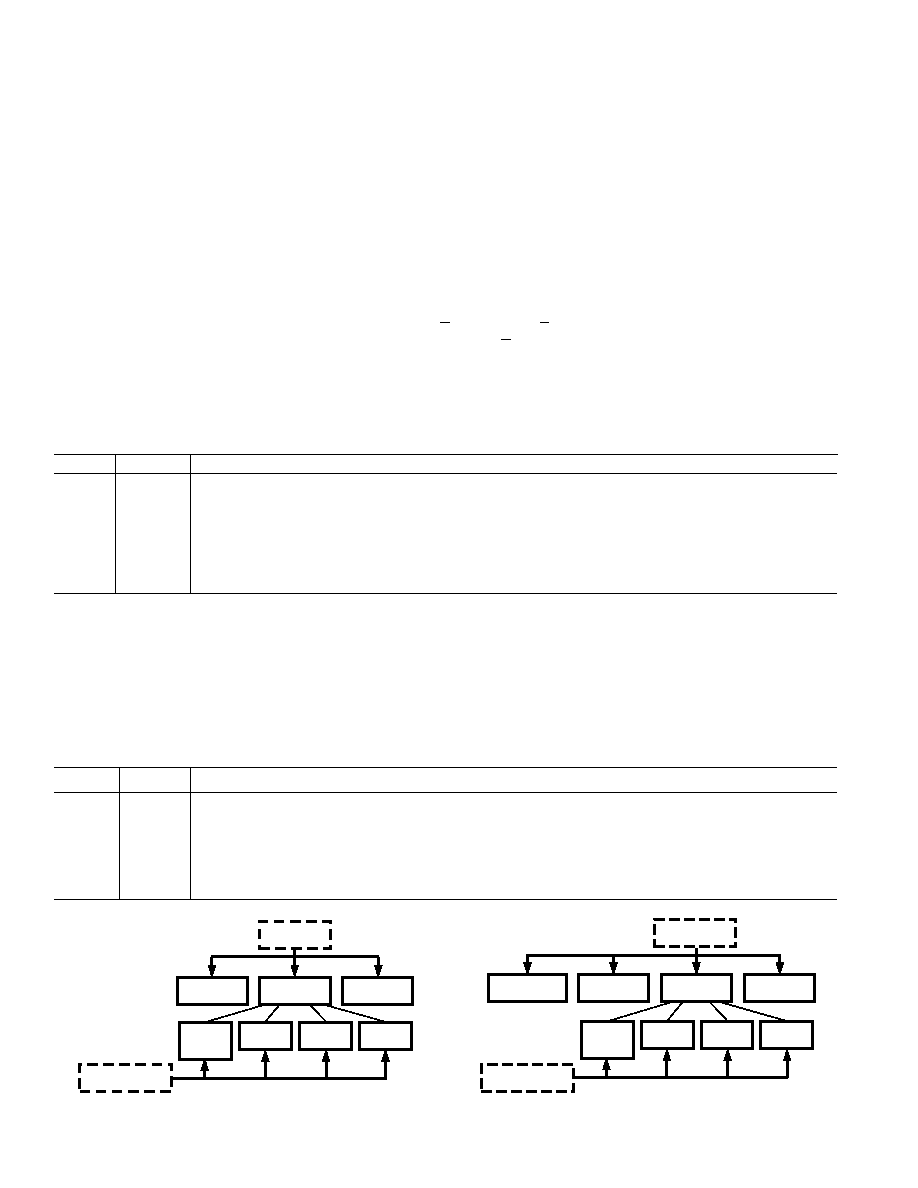
ten to the addressed register. Table I shows the decoding of the address bits, while Figure 2 shows the overall write register hierarchy.
Table I. Write Register Addressing
ADDR1
ADDR0
Comment
0
This combination does not address any register.
0
1
This combination addresses the TEST REGISTER. The 14 LSBs of data are written to the test register.
1
0
This combination addresses the CALIBRATION REGISTERS. The 14 LSBs of data are written to the
selected calibration register.
1
This combination addresses the CONTROL REGISTER. The 14 LSBs of data are written to the control
register.
Reading
To read from the various registers the user must first write to Bits 6 and 7 in the Control Register, RDSLT0 and RDSLT1. These
bits are decoded to determine which register is addressed during a read operation. Table II shows the decoding of the read address
bits while Figure 3 shows the overall read register hierarchy. The power-up status of these bits is 00 so that the default read will be
from the ADC output data register. As with writing to the AD7859/AD7859L either word or byte mode can be used. When reading
from the calibration registers in byte mode, the low byte must be read first.
Once the read selection bits are set in the control register all subsequent read operations that follow are from the selected register un-
til the read selection bits are changed in the control register.
Table II. Read Register Addressing
RDSLT1
RDSLT0
Comment
0
All successive read operations are from the ADC OUTPUT DATA REGISTER. This is the default power-
up setting. There is always four leading zeros when reading from the ADC output data register.
0
1
All successive read operations are from the TEST REGISTER.
1
0
All successive read operations are from the CALIBRATION REGISTERS.
1
All successive read operations are from the STATUS REGISTER.
TEST
REGISTER
CALIBRATION
REGISTERS
STATUS
REGISTER
GAIN (1)
OFFSET (1)
DAC (8)
GAIN (1)
OFFSET (1)
GAIN (1)
01
10
11
00
01
10
11
CALSLT1, CALSLT0
DECODE
ADC OUTPUT
DATA REGISTER
00
RDSLT1, RDSLT0
DECODE
Figure 3. Read Register Hierarchy/Address Decoding
ADDR1, ADDR0
DECODE
TEST
REGISTER
CONTROL
REGISTER
GAIN (1)
OFFSET (1)
DAC (8)
GAIN (1)
OFFSET (1)
GAIN (1)
01
10
11
00
01
10
11
CALSLT1, CALSLT0
DECODE
CALIBRATION
REGISTERS
Figure 2. Write Register Hierarchy/Address Decoding
相关PDF资料 |
PDF描述 |
|---|---|
| VI-23T-IW-S | CONVERTER MOD DC/DC 6.5V 100W |
| VE-22R-MX-F1 | CONVERTER MOD DC/DC 7.5V 75W |
| VI-22W-IW-S | CONVERTER MOD DC/DC 5.5V 100W |
| AD9215BRUZ-65 | IC ADC 10BIT 65MSPS 3V 28TSSOP |
| VI-23T-CU-F4 | CONVERTER MOD DC/DC 6.5V 200W |
相关代理商/技术参数 |
参数描述 |
|---|---|
| AD7861 | 制造商:AD 制造商全称:Analog Devices 功能描述:11-Bit Resolution Simultaneous Sampling A/D Converter |
| AD7861AP | 功能描述:IC ADC 11BIT 4CH 44-PLCC RoHS:否 类别:集成电路 (IC) >> 数据采集 - 模数转换器 系列:- 标准包装:1 系列:- 位数:14 采样率(每秒):83k 数据接口:串行,并联 转换器数目:1 功率耗散(最大):95mW 电压电源:双 ± 工作温度:0°C ~ 70°C 安装类型:通孔 封装/外壳:28-DIP(0.600",15.24mm) 供应商设备封装:28-PDIP 包装:管件 输入数目和类型:1 个单端,双极 |
| AD7861APZ | 功能描述:IC ADC 11BIT 4CHAN 44PLCC RoHS:是 类别:集成电路 (IC) >> 数据采集 - 模数转换器 系列:- 标准包装:1,000 系列:- 位数:12 采样率(每秒):300k 数据接口:并联 转换器数目:1 功率耗散(最大):75mW 电压电源:单电源 工作温度:0°C ~ 70°C 安装类型:表面贴装 封装/外壳:24-SOIC(0.295",7.50mm 宽) 供应商设备封装:24-SOIC 包装:带卷 (TR) 输入数目和类型:1 个单端,单极;1 个单端,双极 |
| AD7862 | 制造商:AD 制造商全称:Analog Devices 功能描述:Simultaneous Sampling Dual 250 kSPS 12-Bit ADC |
| AD7862AN-10 | 功能描述:IC ADC 12BIT DUAL 250KSPS 28-DIP RoHS:否 类别:集成电路 (IC) >> 数据采集 - 模数转换器 系列:- 标准包装:1 系列:- 位数:14 采样率(每秒):83k 数据接口:串行,并联 转换器数目:1 功率耗散(最大):95mW 电压电源:双 ± 工作温度:0°C ~ 70°C 安装类型:通孔 封装/外壳:28-DIP(0.600",15.24mm) 供应商设备封装:28-PDIP 包装:管件 输入数目和类型:1 个单端,双极 |
发布紧急采购,3分钟左右您将得到回复。