- 您现在的位置:买卖IC网 > PDF目录10681 > AD7887WARMZ (Analog Devices Inc)IC ADC 12BIT 2CH SRL 8-MSOP PDF资料下载
参数资料
| 型号: | AD7887WARMZ |
| 厂商: | Analog Devices Inc |
| 文件页数: | 22/24页 |
| 文件大小: | 0K |
| 描述: | IC ADC 12BIT 2CH SRL 8-MSOP |
| 设计资源: | Software Calibrated, 1 MHz to 8 GHz, 70 dB RF Power Measurement System Using AD8318 (CN0150) |
| 标准包装: | 50 |
| 位数: | 12 |
| 采样率(每秒): | 125k |
| 数据接口: | DSP,MICROWIRE?,QSPI?,串行,SPI? |
| 转换器数目: | 1 |
| 功率耗散(最大): | 3.5mW |
| 电压电源: | 单电源 |
| 工作温度: | -40°C ~ 125°C |
| 安装类型: | 表面贴装 |
| 封装/外壳: | 8-TSSOP,8-MSOP(0.118",3.00mm 宽) |
| 供应商设备封装: | 8-MSOP |
| 包装: | 管件 |
| 输入数目和类型: | 2 个单端,单极 |
| 产品目录页面: | 779 (CN2011-ZH PDF) |
AD7887
Rev. D | Page 7 of 24
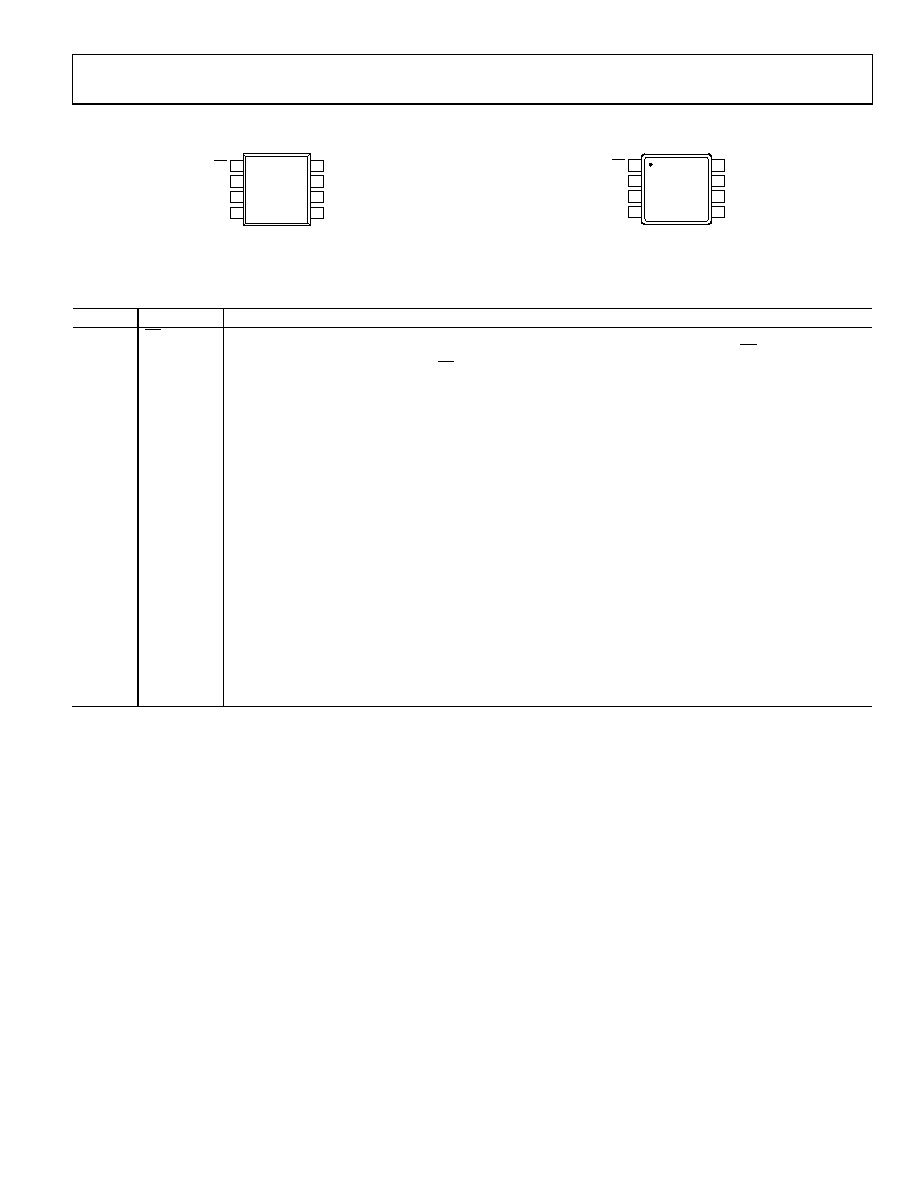
PIN CONFIGURATIONS AND FUNCTION DESCRIPTIONS
CS 1
VDD 2
GND 3
AIN1/VREF 4
SCLK
8
DOUT
7
DIN
6
AIN0
5
AD7887
TOP VIEW
(Not to Scale)
06
19
1-
00
3
CS 1
VDD 2
GND 3
AIN1/VREF 4
SCLK
8
DOUT
7
DIN
6
AIN0
5
AD7887
TOP VIEW
(Not to Scale)
06
19
1-
00
4
Figure 3. SOIC_N Pin Configuration
Figure 4. MSOP Pin Configuration
Table 4. Pin Function Descriptions
Pin No.
Mnemonic
Description
1
CS
Chip Select. Active low logic input. This input provides the dual function of initiating conversions on the AD7887
and also frames the serial data transfer. When the AD7887 operates in its default mode, the CS pin also acts as
the shutdown pin such that with the CS pin high, the AD7887 is in its power-down mode.
2
VDD
Power Supply Input. The VDD range for the AD7887 is from 2.7 V to 5.25 V. When the AD7887 is configured for
two-channel operation, this pin also provides the reference source for the part.
3
GND
Ground Pin. This pin is the ground reference point for all circuitry on the AD7887. In systems with separate AGND
and DGND planes, these planes should be tied together as close as possible to this GND pin. Where this is not
possible, this GND pin should connect to the AGND plane.
4
AIN1/VREF
Analog Input 1/Voltage Reference Input. In single-channel mode, this pin becomes the reference input/output.
In this case, the user can either access the internal 2.5 V reference or overdrive the internal reference with the
voltage applied to this pin. The reference voltage range for an externally applied reference is 1.2 V to VDD. In two-
channel mode, this pin provides the second analog input channel, AIN1. The input voltage range on AIN1 is
0 to VDD.
5
AIN0
Analog Input 0. In single-channel mode, this is the analog input and the input voltage range is 0 to VREF. In dual-
channel mode, it has an analog input range of 0 to VDD.
6
DIN
Data In. Logic Input. Data to be written to the AD7887’s control register is provided on this input and clocked into
the register on the rising edge of SCLK (see the Control Register section). The AD7887 can be operated as a
single-channel, read-only ADC by tying the DIN line permanently to GND.
7
DOUT
Data Out. Logic output. The conversion result from the AD7887 is provided on this output as a serial data stream.
The bits are clocked out on the falling edge of the SCLK input. The data stream consists of four leading zeros
followed by the 12 bits of conversion data, which is provided MSB first.
8
SCLK
Serial Clock. Logic input. SCLK provides the serial clock for accessing data from the part and writing serial data to
the control register. This clock input is also used as the clock source for the AD7887’s conversion process.
相关PDF资料 |
PDF描述 |
|---|---|
| VI-23Y-MX-B1 | CONVERTER MOD DC/DC 3.3V 49.5W |
| AD7791BRMZ | IC ADC 24BIT BUFFERED LP 10MSOP |
| VI-22Z-MY-B1 | CONVERTER MOD DC/DC 2V 20W |
| CS5529-ASZ | IC ADC 16BIT W/6BIT LATCH 20SSOP |
| VI-22Z-MW-B1 | CONVERTER MOD DC/DC 2V 40W |
相关代理商/技术参数 |
参数描述 |
|---|---|
| AD7887WARMZ-RL | 功能描述:IC ADC 12BIT 2CH SRL 8-MSOP RoHS:是 类别:集成电路 (IC) >> 数据采集 - 模数转换器 系列:- 标准包装:1,000 系列:- 位数:16 采样率(每秒):45k 数据接口:串行 转换器数目:2 功率耗散(最大):315mW 电压电源:模拟和数字 工作温度:0°C ~ 70°C 安装类型:表面贴装 封装/外壳:28-SOIC(0.295",7.50mm 宽) 供应商设备封装:28-SOIC W 包装:带卷 (TR) 输入数目和类型:2 个单端,单极 |
| AD7888AR | 制造商:Analog Devices 功能描述:ADC Single SAR 125ksps 12-bit Serial 16-Pin SOIC N 制造商:Analog Devices 功能描述:IC 12BIT ADC 8CH MICROPOWER 7888 |
| AD7888AR-REEL | 制造商:Analog Devices 功能描述:ADC Single SAR 125ksps 12-bit Serial 16-Pin SOIC N T/R |
| AD7888AR-REEL7 | 制造商:Analog Devices 功能描述:ADC Single SAR 125ksps 12-bit Serial 16-Pin SOIC N T/R |
| AD7888ARU | 功能描述:IC ADC 12BIT 8CH 125KSPS 16TSSOP RoHS:否 类别:集成电路 (IC) >> 数据采集 - 模数转换器 系列:- 标准包装:1,000 系列:- 位数:12 采样率(每秒):300k 数据接口:并联 转换器数目:1 功率耗散(最大):75mW 电压电源:单电源 工作温度:0°C ~ 70°C 安装类型:表面贴装 封装/外壳:24-SOIC(0.295",7.50mm 宽) 供应商设备封装:24-SOIC 包装:带卷 (TR) 输入数目和类型:1 个单端,单极;1 个单端,双极 |
发布紧急采购,3分钟左右您将得到回复。