- 您现在的位置:买卖IC网 > PDF目录10681 > AD7887WARMZ (Analog Devices Inc)IC ADC 12BIT 2CH SRL 8-MSOP PDF资料下载
参数资料
| 型号: | AD7887WARMZ |
| 厂商: | Analog Devices Inc |
| 文件页数: | 4/24页 |
| 文件大小: | 0K |
| 描述: | IC ADC 12BIT 2CH SRL 8-MSOP |
| 设计资源: | Software Calibrated, 1 MHz to 8 GHz, 70 dB RF Power Measurement System Using AD8318 (CN0150) |
| 标准包装: | 50 |
| 位数: | 12 |
| 采样率(每秒): | 125k |
| 数据接口: | DSP,MICROWIRE?,QSPI?,串行,SPI? |
| 转换器数目: | 1 |
| 功率耗散(最大): | 3.5mW |
| 电压电源: | 单电源 |
| 工作温度: | -40°C ~ 125°C |
| 安装类型: | 表面贴装 |
| 封装/外壳: | 8-TSSOP,8-MSOP(0.118",3.00mm 宽) |
| 供应商设备封装: | 8-MSOP |
| 包装: | 管件 |
| 输入数目和类型: | 2 个单端,单极 |
| 产品目录页面: | 779 (CN2011-ZH PDF) |
AD7887
Rev. D | Page 12 of 24
ANALOG INPUT
Figure 12 shows an equivalent circuit of the analog input
structure of the AD7887. The two diodes, D1 and D2, provide
ESD protection for the analog inputs. Care must be taken to
ensure that the analog input signal never exceed the supply rails
by more than 200 mV. Exceeding this value causes the diodes
to become forward biased and to start conducting into the
substrate. The maximum current these diodes can conduct
without causing irreversible damage to the part is 20 mA.
However, it is worth noting that a small amount of current
(1 mA) being conducted into the substrate due to an
overvoltage on an unselected channel can cause inaccurate
conversions on a selected channel. Capacitor C1 in Figure 12 is
typically about 4 pF and can primarily be attributed to pin
capacitance. Resistor R1 is a lumped component made up of the
on resistance of a multiplexer and a switch. This resistor is
typically about 100 Ω. Capacitor C2 is the ADC sampling
capacitor and typically has a capacitance of 20 pF.
Note that the analog input capacitance seen when in track mode
is typically 38 pF, whereas in hold mode it is typically 4 pF.
VIN
VDD
D2
R1
C1
4pF
CONVERSION PHASE—SWITCH OPEN
TRACK PHASE—SWITCH CLOSED
D1
C2
20pF
06
19
1-
01
2
Figure 12. Equivalent Analog Input Circuit
For ac applications, removing high frequency components from
the analog input signal is recommended by use of an RC
low-pass filter on the relevant analog input pin. In applications
where harmonic distortion and signal-to-noise ratio are critical,
the analog input should be driven from a low impedance
source. Large source impedances will significantly affect the ac
performance of the ADC. This may necessitate the use of an
input buffer amplifier. The choice of op amp is a function of the
particular application.
When no amplifier is used to drive the analog input, the source
impedance should be limited to low values. The maximum
source impedance depends on the amount of total harmonic
distortion (THD) that can be tolerated. The THD increases as
the source impedance increases and performance degrades.
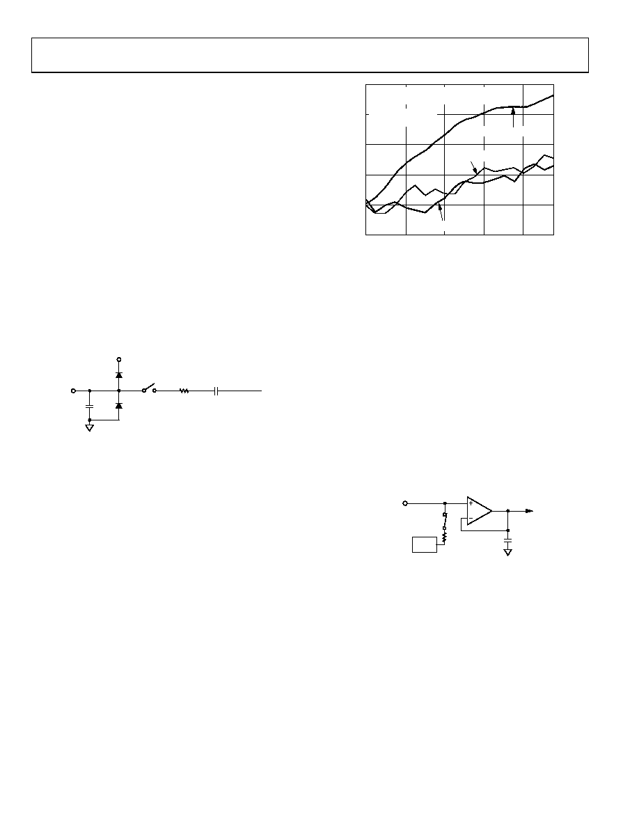
Figure 13 shows a graph of the total harmonic distortion vs. the
analog input signal frequency for different source impedances.
INPUT FREQUENCY (kHz)
–90
4
1
.
2
4
5
1
.
0
TH
D
(
d
B
)
10.89
31.59
21.14
–85
–80
–75
–70
–65
49.86
THD vs. FREQUENCY FOR DIFFERENT
SOURCE IMPEDANCES
VDD = 5V
5V EXT REFERENCE
RIN = 1k, CIN = 100pF
RIN = 50, CIN = 2.2nF
RIN = 10, CIN = 10nF
0
61
91
-0
13
Figure 13. THD vs. Analog Input Frequency
On-Chip Reference
The AD7887 has an on-chip 2.5 V reference. This reference can
be enabled or disabled by clearing or setting the REF bit in the
control register, respectively. If the on-chip reference is to be used
externally in a system, it must be buffered before it is applied
elsewhere. If an external reference is applied to the device, the
internal reference is automatically overdriven. However, it is
advised to disable the internal reference by setting the REF bit
in the control register when an external reference is applied in
order to obtain optimum performance from the device. When
the internal reference is disabled, SW1, shown in Figure 14,
opens and the input impedance seen at the AIN1/VREF pin is the
input impedance of the reference buffer, which is in the region
of gigaohms. When the internal reference is enabled, the input
impedance seen at the pin is typically 10 kΩ. When the AD7887
is operated in two-channel mode, the reference is taken from
VDD internally, not from the on-chip 2.5 V reference.
2.5V
10k
SW1
AIN1/VREF
06
191
-01
4
Figure 14. On-Chip Reference Circuitry
相关PDF资料 |
PDF描述 |
|---|---|
| VI-23Y-MX-B1 | CONVERTER MOD DC/DC 3.3V 49.5W |
| AD7791BRMZ | IC ADC 24BIT BUFFERED LP 10MSOP |
| VI-22Z-MY-B1 | CONVERTER MOD DC/DC 2V 20W |
| CS5529-ASZ | IC ADC 16BIT W/6BIT LATCH 20SSOP |
| VI-22Z-MW-B1 | CONVERTER MOD DC/DC 2V 40W |
相关代理商/技术参数 |
参数描述 |
|---|---|
| AD7887WARMZ-RL | 功能描述:IC ADC 12BIT 2CH SRL 8-MSOP RoHS:是 类别:集成电路 (IC) >> 数据采集 - 模数转换器 系列:- 标准包装:1,000 系列:- 位数:16 采样率(每秒):45k 数据接口:串行 转换器数目:2 功率耗散(最大):315mW 电压电源:模拟和数字 工作温度:0°C ~ 70°C 安装类型:表面贴装 封装/外壳:28-SOIC(0.295",7.50mm 宽) 供应商设备封装:28-SOIC W 包装:带卷 (TR) 输入数目和类型:2 个单端,单极 |
| AD7888AR | 制造商:Analog Devices 功能描述:ADC Single SAR 125ksps 12-bit Serial 16-Pin SOIC N 制造商:Analog Devices 功能描述:IC 12BIT ADC 8CH MICROPOWER 7888 |
| AD7888AR-REEL | 制造商:Analog Devices 功能描述:ADC Single SAR 125ksps 12-bit Serial 16-Pin SOIC N T/R |
| AD7888AR-REEL7 | 制造商:Analog Devices 功能描述:ADC Single SAR 125ksps 12-bit Serial 16-Pin SOIC N T/R |
| AD7888ARU | 功能描述:IC ADC 12BIT 8CH 125KSPS 16TSSOP RoHS:否 类别:集成电路 (IC) >> 数据采集 - 模数转换器 系列:- 标准包装:1,000 系列:- 位数:12 采样率(每秒):300k 数据接口:并联 转换器数目:1 功率耗散(最大):75mW 电压电源:单电源 工作温度:0°C ~ 70°C 安装类型:表面贴装 封装/外壳:24-SOIC(0.295",7.50mm 宽) 供应商设备封装:24-SOIC 包装:带卷 (TR) 输入数目和类型:1 个单端,单极;1 个单端,双极 |
发布紧急采购,3分钟左右您将得到回复。