- 您现在的位置:买卖IC网 > PDF目录10681 > AD7887WARMZ (Analog Devices Inc)IC ADC 12BIT 2CH SRL 8-MSOP PDF资料下载
参数资料
| 型号: | AD7887WARMZ |
| 厂商: | Analog Devices Inc |
| 文件页数: | 5/24页 |
| 文件大小: | 0K |
| 描述: | IC ADC 12BIT 2CH SRL 8-MSOP |
| 设计资源: | Software Calibrated, 1 MHz to 8 GHz, 70 dB RF Power Measurement System Using AD8318 (CN0150) |
| 标准包装: | 50 |
| 位数: | 12 |
| 采样率(每秒): | 125k |
| 数据接口: | DSP,MICROWIRE?,QSPI?,串行,SPI? |
| 转换器数目: | 1 |
| 功率耗散(最大): | 3.5mW |
| 电压电源: | 单电源 |
| 工作温度: | -40°C ~ 125°C |
| 安装类型: | 表面贴装 |
| 封装/外壳: | 8-TSSOP,8-MSOP(0.118",3.00mm 宽) |
| 供应商设备封装: | 8-MSOP |
| 包装: | 管件 |
| 输入数目和类型: | 2 个单端,单极 |
| 产品目录页面: | 779 (CN2011-ZH PDF) |
AD7887
Rev. D | Page 13 of 24
POWER-DOWN OPTIONS
The AD7887 provides flexible power management to allow
the user to achieve the best power performance for a given
throughput rate.
The power management options are selected by programming
the power management bits (that is, PM1 and PM0) in the
control register. Table 6 summarizes the available options.
When the power management bits are programmed for either
of the auto power-down modes, the part enters power-down
mode on the 16th rising SCLK edge after the falling edge of CS.
The first falling SCLK edge after the CS falling edge causes the
part to power up again. When the AD7887 is in Mode 1, that is,
PM1 = PM0 = 0, the part enters shutdown on the rising edge of
CS and power up from shutdown on the falling edge of CS. If
CS is brought high during the conversion in this mode, the part
immediately enters shutdown.
Power-Up Times
The AD7887 has an approximate 1 μs power-up time when
powering up from standby or when using an external reference.
When VDD is first connected the AD7887 powers up in Mode 1,
that is, PM1 = PM0 = 0. The part is put into shutdown on the
rising edge of CS in this mode. A subsequent power-up from
shutdown takes approximately 5 μs. The AD7887 wake-up time
is very short in the autostandby mode; therefore, it is possible to
wake up the part and carry out a valid conversion in the same
read/write operation.
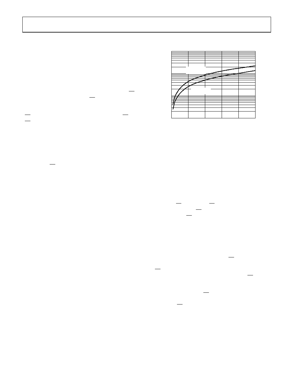
POWER VS. THROUGHPUT RATE
By operating the AD7887 in autoshutdown mode, autostandby
mode, or Mode 1, the average power consumption of the
AD7887 decreases at lower throughput rates. Figure 15 shows
how as the throughput rate is reduced, the device remains in its
power-down state longer and the average power consumption
over time drops accordingly.
For example, if the AD7887 is operated in a continuous sampling
mode with a throughput rate of 10 kSPS and a SCLK of 2 MHz
(VDD = 5 V), PM1 = 1 and PM0 = 0, that is, the device is in auto-
shutdown mode, and the on-chip reference is used, the power
consumption is calculated as follows: The power dissipation
during normal operation is 3.5 mW (VDD = 5 V). If the power-up
time is 5 μs and the remaining conversion plus acquisition time
AD7887 can be said to dissipate 3.5 mW for 12.75 μs during
each conversion cycle. If the throughput rate is 10 kSPS, the
cycle time is 100 μs and the average power dissipated during
each cycle is (12.75/100) × (3.5 mW) = 446.25 μW. If VDD = 3 V,
SCLK = 2 MHz, and the device is in autoshutdown mode using the
on-chip reference, the power dissipation during normal operation
is 2.1 mW. The AD7887 can now be said to dissipate 2.1 mW
for 12.75 μs during each conversion cycle. With a throughput
rate of 10 kSPS, the average power dissipated during each cycle
is (12.75/100) × (2.1 mW) = 267.75 μW. Figure 15 shows the
power vs. throughput rate for automatic shutdown with both
5 V and 3 V supplies.
THROUGHPUT RATE (kSPS)
10
0
P
O
WE
R
(
m
W)
1
10
0.1
0.01
VDD = 5V
SCLK = 2MHz
VDD = 3V
SCLK = 2MHz
20
50
40
30
06
19
1-
01
5
Figure 15. Power vs. Throughput Rate
MODES OF OPERATION
The AD7887 has several modes of operation that are designed
to provide flexible power management options. These options
can be chosen to optimize the power dissipation/throughput
rate ratio for differing application requirements. The modes of
operation are controlled by the PM1 and PM0 bits of the control
register, as previously outlined in Table 6. For read-only operation
of the AD7887, the default mode of all 0s in the control register
can be set up by tying the DIN line permanently low.
Mode 1 (PM1 = 0, PM0 = 0)
This mode allows the user to control the powering down of the
part via the CS pin. Whenever CS is low, the AD7887 is fully
powered up; whenever CS is high, the AD7887 is in full
shutdown. When CS goes from high to low, all on-chip circuitry
starts to power up. It takes approximately 5 μs for the AD7887
internal circuitry to be fully powered up. As a result, a
conversion (or sample-and-hold acquisition) should not be
initiated during this 5 μs.
Figure 16 shows a general diagram of the operation of the
AD7887 in this mode. The input signal is sampled on the
second rising edge of SCLK following the CS falling edge. The
user should ensure that 5 μs elapses between the falling edge of
CS and the second rising edge of SCLK. In microcontroller
applications, this is readily achievable by driving the CS input
from one of the port lines and ensuring that the serial data read
(from the microcontrollers serial port) is not initiated for 5 μs.
In DSP applications, where CS is generally derived from the
serial frame synchronization line, it is usually not possible to
separate the CS falling edge and second SCLK rising edge by up
to 5 μs without affecting the speed of the rest of the serial clock.
Therefore, the user must write to the control register to exit this
mode and (by writing PM1 = 0 and PM0 = 1) put the part into
Mode 2, that is, normal mode. A second conversion needs to be
initiated when the part is powered up to get a conversion result.
The write operation that takes place in conjunction with this
相关PDF资料 |
PDF描述 |
|---|---|
| VI-23Y-MX-B1 | CONVERTER MOD DC/DC 3.3V 49.5W |
| AD7791BRMZ | IC ADC 24BIT BUFFERED LP 10MSOP |
| VI-22Z-MY-B1 | CONVERTER MOD DC/DC 2V 20W |
| CS5529-ASZ | IC ADC 16BIT W/6BIT LATCH 20SSOP |
| VI-22Z-MW-B1 | CONVERTER MOD DC/DC 2V 40W |
相关代理商/技术参数 |
参数描述 |
|---|---|
| AD7887WARMZ-RL | 功能描述:IC ADC 12BIT 2CH SRL 8-MSOP RoHS:是 类别:集成电路 (IC) >> 数据采集 - 模数转换器 系列:- 标准包装:1,000 系列:- 位数:16 采样率(每秒):45k 数据接口:串行 转换器数目:2 功率耗散(最大):315mW 电压电源:模拟和数字 工作温度:0°C ~ 70°C 安装类型:表面贴装 封装/外壳:28-SOIC(0.295",7.50mm 宽) 供应商设备封装:28-SOIC W 包装:带卷 (TR) 输入数目和类型:2 个单端,单极 |
| AD7888AR | 制造商:Analog Devices 功能描述:ADC Single SAR 125ksps 12-bit Serial 16-Pin SOIC N 制造商:Analog Devices 功能描述:IC 12BIT ADC 8CH MICROPOWER 7888 |
| AD7888AR-REEL | 制造商:Analog Devices 功能描述:ADC Single SAR 125ksps 12-bit Serial 16-Pin SOIC N T/R |
| AD7888AR-REEL7 | 制造商:Analog Devices 功能描述:ADC Single SAR 125ksps 12-bit Serial 16-Pin SOIC N T/R |
| AD7888ARU | 功能描述:IC ADC 12BIT 8CH 125KSPS 16TSSOP RoHS:否 类别:集成电路 (IC) >> 数据采集 - 模数转换器 系列:- 标准包装:1,000 系列:- 位数:12 采样率(每秒):300k 数据接口:并联 转换器数目:1 功率耗散(最大):75mW 电压电源:单电源 工作温度:0°C ~ 70°C 安装类型:表面贴装 封装/外壳:24-SOIC(0.295",7.50mm 宽) 供应商设备封装:24-SOIC 包装:带卷 (TR) 输入数目和类型:1 个单端,单极;1 个单端,双极 |
发布紧急采购,3分钟左右您将得到回复。