- 您现在的位置:买卖IC网 > PDF目录10679 > AD7888ARUZ-REEL7 (Analog Devices Inc)IC ADC 12BIT SRL 125KSPS 16TSSOP PDF资料下载
参数资料
| 型号: | AD7888ARUZ-REEL7 |
| 厂商: | Analog Devices Inc |
| 文件页数: | 13/17页 |
| 文件大小: | 0K |
| 描述: | IC ADC 12BIT SRL 125KSPS 16TSSOP |
| 标准包装: | 1 |
| 位数: | 12 |
| 采样率(每秒): | 125k |
| 数据接口: | DSP,MICROWIRE?,QSPI?,串行,SPI? |
| 转换器数目: | 1 |
| 功率耗散(最大): | 3.5mW |
| 电压电源: | 单电源 |
| 工作温度: | -40°C ~ 105°C |
| 安装类型: | 表面贴装 |
| 封装/外壳: | 16-TSSOP(0.173",4.40mm 宽) |
| 供应商设备封装: | 16-TSSOP |
| 包装: | 标准包装 |
| 输入数目和类型: | 8 个单端,单极 |
| 其它名称: | AD7888ARUZ-REEL7DKR |
AD7888
–5–
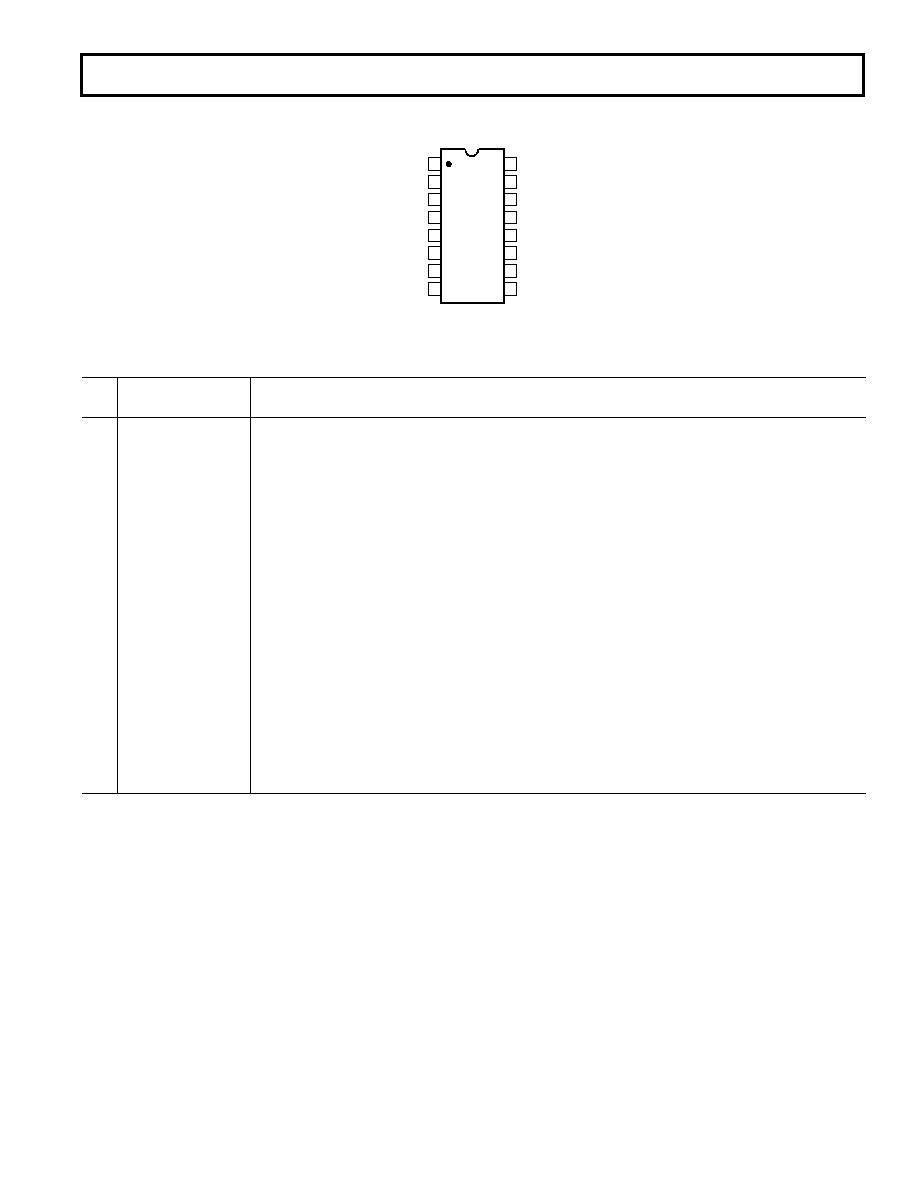
PIN CONFIGURATIONS
SOIC AND TSSOP
TOP VIEW
(Not to Scale)
16
15
14
13
12
11
10
9
1
2
3
4
5
6
7
8
CS
REF IN/REF OUT
VDD
AGND
AIN1
AIN2
AIN3
AIN4
SCLK
DOUT
DIN
AGND
AIN8
AIN7
AIN6
AIN5
AD7888
PIN FUNCTION DESCRIPTIONS
Pin
No.
Mnemonic
Function
1
CS
Chip Select. Active low logic input. This input provides the dual function of initiating conversions on
the AD7888 and also frames the serial data transfer.
2
REF IN/REF OUT
Reference Input/Output. The on-chip reference is available on this pin for use external to the AD7888.
Alternatively, the internal reference can be disabled and an external reference applied to this input.
The voltage range for the external reference is from 1.2 V to VDD.
3VDD
Power Supply Input. The VDD range for the AD7888 is from 2.7 V to 5.25 V.
4, 13
AGND
Analog Ground. Ground reference point for all circuitry on the AD7888. All analog input signals and
any external reference signals should be referred to this AGND voltage. Both of these pins should
connect to the AGND plane of a system.
5–12
AIN1–AIN8
Analog Input 1 through Analog Input 8. Eight single-ended analog input channels that are multiplexed
into the on-chip track/hold. The analog input channel to be converted is selected by using the ADD0
through ADD2 bits of the Control Register. The input range for all input channels is 0 to VREF. Any
unused input channels should be connected to AGND to avoid noise pickup.
14
DIN
Data In. Logic Input. Data to be written to the AD7888’s Control Register is provided on this input
and is clocked into the register on the rising edge of SCLK (see Control Register section).
15
DOUT
Data Out. Logic Output. The conversion result from the AD7888 is provided on this output as a serial
data stream. The bits are clocked out on the falling edge of the SCLK input. The data stream consists
of four leading zeros followed by the 12 bits of conversion data, which is provided MSB first.
16
SCLK
Serial Clock. Logic Input. SCLK provides the serial clock for accessing data from the part and writing
serial data to the Control Register. This clock input is also used as the clock source for the AD7888’s
conversion process.
REV. C
相关PDF资料 |
PDF描述 |
|---|---|
| MC10H115PG | IC RECEIVER QUAD LINE ECL 16DIP |
| ADCMP562BRQ | IC COMPARATOR PECL DUAL 20QSOP |
| ADCMP551BRQ | IC COMPARATOR PECL/LVPECL 16QSOP |
| AD790JR-REEL | IC COMPARATOR PREC W/LATCH 8SOIC |
| LT1016IS8 | IC COMPARATOR 10NS HI-SPD 8-SOIC |
相关代理商/技术参数 |
参数描述 |
|---|---|
| AD7888ARZ | 功能描述:IC ADC 12BIT 8CH SRL 16-SOIC RoHS:是 类别:集成电路 (IC) >> 数据采集 - 模数转换器 系列:- 标准包装:1 系列:microPOWER™ 位数:8 采样率(每秒):1M 数据接口:串行,SPI? 转换器数目:1 功率耗散(最大):- 电压电源:模拟和数字 工作温度:-40°C ~ 125°C 安装类型:表面贴装 封装/外壳:24-VFQFN 裸露焊盘 供应商设备封装:24-VQFN 裸露焊盘(4x4) 包装:Digi-Reel® 输入数目和类型:8 个单端,单极 产品目录页面:892 (CN2011-ZH PDF) 其它名称:296-25851-6 |
| AD7888ARZ-REEL | 功能描述:IC ADC 12BIT 8CH SRL 16-SOIC RoHS:是 类别:集成电路 (IC) >> 数据采集 - 模数转换器 系列:- 产品培训模块:Lead (SnPb) Finish for COTS Obsolescence Mitigation Program 标准包装:2,500 系列:- 位数:12 采样率(每秒):3M 数据接口:- 转换器数目:- 功率耗散(最大):- 电压电源:- 工作温度:- 安装类型:表面贴装 封装/外壳:SOT-23-6 供应商设备封装:SOT-23-6 包装:带卷 (TR) 输入数目和类型:- |
| AD7888ARZ-REEL7 | 功能描述:IC ADC 12BIT 8CH SRL 16-SOIC RoHS:是 类别:集成电路 (IC) >> 数据采集 - 模数转换器 系列:- 标准包装:1,000 系列:- 位数:16 采样率(每秒):45k 数据接口:串行 转换器数目:2 功率耗散(最大):315mW 电压电源:模拟和数字 工作温度:0°C ~ 70°C 安装类型:表面贴装 封装/外壳:28-SOIC(0.295",7.50mm 宽) 供应商设备封装:28-SOIC W 包装:带卷 (TR) 输入数目和类型:2 个单端,单极 |
| AD7888BR | 制造商:Analog Devices 功能描述:ADC Single SAR 125ksps 12-bit Serial 16-Pin SOIC N |
| AD7888BR-REEL | 功能描述:IC ADC 12BIT 8CHAN SRL 16SOIC RoHS:否 类别:集成电路 (IC) >> 数据采集 - 模数转换器 系列:- 标准包装:1,000 系列:- 位数:16 采样率(每秒):45k 数据接口:串行 转换器数目:2 功率耗散(最大):315mW 电压电源:模拟和数字 工作温度:0°C ~ 70°C 安装类型:表面贴装 封装/外壳:28-SOIC(0.295",7.50mm 宽) 供应商设备封装:28-SOIC W 包装:带卷 (TR) 输入数目和类型:2 个单端,单极 |
发布紧急采购,3分钟左右您将得到回复。