- 您现在的位置:买卖IC网 > PDF目录9713 > AD7889ACBZ-RL (Analog Devices Inc)IC ADC 12BIT CTRLR TOUCH 12WLCSP PDF资料下载
参数资料
| 型号: | AD7889ACBZ-RL |
| 厂商: | Analog Devices Inc |
| 文件页数: | 25/41页 |
| 文件大小: | 0K |
| 描述: | IC ADC 12BIT CTRLR TOUCH 12WLCSP |
| 产品变化通告: | 8mm Carrier Tape Changes 28/Feb/2012 |
| 标准包装: | 10,000 |
| 类型: | 电阻 |
| 触摸面板接口: | 4 线 |
| 输入数/键: | 1 TSC |
| 分辨率(位): | 12 b |
| 数据接口: | 串行,SPI? |
| 数据速率/采样率 (SPS,BPS): | 105k |
| 电压基准: | 外部 |
| 电源电压: | 1.6 V ~ 3.6 V |
| 电流 - 电源: | 10nA |
| 工作温度: | -40°C ~ 85°C |
| 安装类型: | 表面贴装 |
| 封装/外壳: | 12-UFBGA,WLCSP |
| 供应商设备封装: | 12-WLCSP |
| 包装: | 带卷 (TR) |
第1页第2页第3页第4页第5页第6页第7页第8页第9页第10页第11页第12页第13页第14页第15页第16页第17页第18页第19页第20页第21页第22页第23页第24页当前第25页第26页第27页第28页第29页第30页第31页第32页第33页第34页第35页第36页第37页第38页第39页第40页第41页
AD7879/AD7889
Rev. C | Page 30 of 40
INTERRUPTS
The AD7879/AD7889 have a dual function interrupt output,
INT, as well as a pen-down interrupt, PENIRQ. The INT output
can be configured as a data available interrupt (DAV), as an
out-of-limit interrupt (INT), or as a GPIO interrupt.
DAV—Data Available Interrupt
The behavior of the interrupt output is controlled by Bit 13 in
Control Register 3. In default mode (Bit 13 = 0), INT operates
as a data available interrupt (DAV). When the AD7879/AD7889
finish a conversion or a conversion sequence, the interrupt is
asserted to let the host know that new ADC data is available in
the result registers.
While the ADC is idle or is converting, DAV is high. When the
ADC has finished converting and new data has been written to
the result registers, DAV goes low. Reading the result registers
resets DAV to a high condition. DAV is also reset if a new con-
version is started by the AD7879/AD7889 because the timer
expired. The host should read the result registers only when
DAV is low. To ensure correct operation of the DAV mode
when using the SPI interface, it is necessary to write 0x0000
to Register 0x81 after a set of register reads. This clears the
internal data read signal.
ADC
CONVERTING
SETUP
BY HOST
IDLE
NEW DATA
AVAILABLE
HOST READS
RESULTS
IDLE
tCONV
AD7879/
AD7889
STATUS
DAV
07667-
034
Figure 35. Operation of DAV Output
When the on-board timer is programmed to perform automatic
conversions, limited time is available to the host to read the
result registers before another sequence of conversions begins.
The DAV signal is reset high when the timer expires, and the
host should not access the result registers while DAV is high.
INT—Out-of-Limit Interrupt
The INT pin operates as an alarm or interrupt output when
Bit 13 in Control Register 3 (Address 0x03) is set to 1. The
output goes low if any one of the interrupt sources is asserted.
The results of high and low limit comparisons on the AUX,
VBAT, and TEMP channels are interrupt sources. An out-of-
limit comparison sets a status bit in the interrupt register. A
separate status bit for the high limit and the low limit on each
channel indicates which limit was exceeded. The interrupt
sources can be masked by setting the corresponding enable bit
in this register to 1. There is one enable bit per channel.
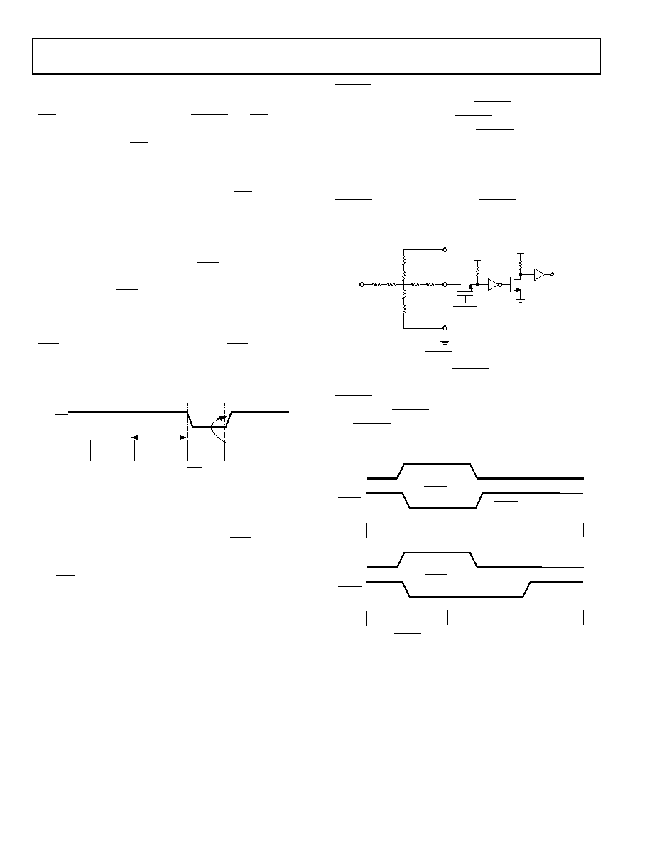
PENIRQ—Pen Interrupt
The pen interrupt request output (PENIRQ) goes low whenever
the screen is touched and the PENIRQ enable bit is set to 0
(Control Register 1, Bit 15). When PENIRQ enable is set to 1,
the pen interrupt request output is disabled.
The pen interrupt equivalent output circuitry is shown in
Figure 36. This digital logic output has an internal 50 k pull-
up resistor, so it does not need an external pull-up. The
PENIRQ output idles high, and the PENIRQ circuitry is always
enabled in master mode (ADC mode = 11), except during
conversions.
07667-
035
X+
TOUCH
SCREEN
Y+
50k
Y–
X–
PENIRQ
ENABLE
PENIRQ
VCC
Figure 36. PENIRQ Output Equivalent Circuit
When the screen is touched, PENIRQ goes low. This generates
an interrupt request to the host. When the screen touch ends,
PENIRQ immediately goes high if the ADC is idle. If the ADC
is converting, PENIRQ goes high when the ADC becomes idle.
The PENIRQ operation for these two conditions is shown in
07667-
036
SCREEN
PENIRQ
ADC
STATUS
TOUCHED
NOT
TOUCHED
NOT
TOUCHED
NOT
TOUCHED
NOT
TOUCHED
ADC IDLE
SCREEN
PENIRQ
ADC
STATUS
TOUCHED
ADC IDLE
ADC
CONVERTING
ADC IDLE
RELEASE NOT
DETECTED
PENIRQ
DETECTS
RELEASE
PENIRQ
DETECTS
RELEASE
PENIRQ
DETECTS
TOUCH
PENIRQ
DETECTS
TOUCH
Figure 37. PENIRQ Operation for ADC Idle and ADC Converting
相关PDF资料 |
PDF描述 |
|---|---|
| AD7889-1ACBZ-RL | IC ADC 12BIT CTRLR TOUCH 12WLCSP |
| VE-BTV-IV-B1 | CONVERTER MOD DC/DC 5.8V 150W |
| VE-BT0-IV-B1 | CONVERTER MOD DC/DC 5V 150W |
| VE-B4H-IV-B1 | CONVERTER MOD DC/DC 52V 150W |
| AD7879-1ACPZ-RL | IC ADC 12BIT CTLR TOUCH 16LFCSP |
相关代理商/技术参数 |
参数描述 |
|---|---|
| AD7890ACHIPS-2 | 功能描述:Data Acquisition System (DAS) 12 bit 117k SPI Die 制造商:analog devices inc. 系列:- 包装:管件 零件状态:上次购买时间 类型:数据采集系统(DAS) 分辨率(位):12 b 采样率(每秒):117k 数据接口:SPI 电压源:单电源 电压 - 电源:5V 工作温度:-40°C ~ 85°C 安装类型:表面贴装 封装/外壳:模具 供应商器件封装:模具 标准包装:1 |
| AD7890AN-10 | 功能描述:IC DAS 12BIT 8CH 24-DIP RoHS:否 类别:集成电路 (IC) >> 数据采集 - ADCs/DAC - 专用型 系列:- 产品培训模块:Lead (SnPb) Finish for COTS Obsolescence Mitigation Program 标准包装:50 系列:- 类型:数据采集系统(DAS) 分辨率(位):16 b 采样率(每秒):21.94k 数据接口:MICROWIRE?,QSPI?,串行,SPI? 电压电源:模拟和数字 电源电压:1.8 V ~ 3.6 V 工作温度:-40°C ~ 85°C 安装类型:表面贴装 封装/外壳:40-WFQFN 裸露焊盘 供应商设备封装:40-TQFN-EP(6x6) 包装:托盘 |
| AD7890AN-2 | 功能描述:IC DAS 12BIT 8CH 24-DIP RoHS:否 类别:集成电路 (IC) >> 数据采集 - ADCs/DAC - 专用型 系列:- 产品培训模块:Lead (SnPb) Finish for COTS Obsolescence Mitigation Program 标准包装:50 系列:- 类型:数据采集系统(DAS) 分辨率(位):16 b 采样率(每秒):21.94k 数据接口:MICROWIRE?,QSPI?,串行,SPI? 电压电源:模拟和数字 电源电压:1.8 V ~ 3.6 V 工作温度:-40°C ~ 85°C 安装类型:表面贴装 封装/外壳:40-WFQFN 裸露焊盘 供应商设备封装:40-TQFN-EP(6x6) 包装:托盘 |
| AD7890AN-4 | 制造商:Analog Devices 功能描述:ADC Single SAR 117ksps 12-bit Serial 24-Pin PDIP 制造商:Rochester Electronics LLC 功能描述:8 CHANNEL,SERIAL A/D IC - Bulk |
| AD7890ANZ-10 | 功能描述:IC DAS 12BIT 8CH 24-DIP RoHS:是 类别:集成电路 (IC) >> 数据采集 - ADCs/DAC - 专用型 系列:- 产品培训模块:Lead (SnPb) Finish for COTS Obsolescence Mitigation Program 标准包装:50 系列:- 类型:数据采集系统(DAS) 分辨率(位):16 b 采样率(每秒):21.94k 数据接口:MICROWIRE?,QSPI?,串行,SPI? 电压电源:模拟和数字 电源电压:1.8 V ~ 3.6 V 工作温度:-40°C ~ 85°C 安装类型:表面贴装 封装/外壳:40-WFQFN 裸露焊盘 供应商设备封装:40-TQFN-EP(6x6) 包装:托盘 |
发布紧急采购,3分钟左右您将得到回复。