- 您现在的位置:买卖IC网 > PDF目录9713 > AD7889ACBZ-RL (Analog Devices Inc)IC ADC 12BIT CTRLR TOUCH 12WLCSP PDF资料下载
参数资料
| 型号: | AD7889ACBZ-RL |
| 厂商: | Analog Devices Inc |
| 文件页数: | 6/41页 |
| 文件大小: | 0K |
| 描述: | IC ADC 12BIT CTRLR TOUCH 12WLCSP |
| 产品变化通告: | 8mm Carrier Tape Changes 28/Feb/2012 |
| 标准包装: | 10,000 |
| 类型: | 电阻 |
| 触摸面板接口: | 4 线 |
| 输入数/键: | 1 TSC |
| 分辨率(位): | 12 b |
| 数据接口: | 串行,SPI? |
| 数据速率/采样率 (SPS,BPS): | 105k |
| 电压基准: | 外部 |
| 电源电压: | 1.6 V ~ 3.6 V |
| 电流 - 电源: | 10nA |
| 工作温度: | -40°C ~ 85°C |
| 安装类型: | 表面贴装 |
| 封装/外壳: | 12-UFBGA,WLCSP |
| 供应商设备封装: | 12-WLCSP |
| 包装: | 带卷 (TR) |
第1页第2页第3页第4页第5页当前第6页第7页第8页第9页第10页第11页第12页第13页第14页第15页第16页第17页第18页第19页第20页第21页第22页第23页第24页第25页第26页第27页第28页第29页第30页第31页第32页第33页第34页第35页第36页第37页第38页第39页第40页第41页
AD7879/AD7889
Rev. C | Page 13 of 40
THEORY OF OPERATION
The AD7879/AD7889 are a complete 12-bit data acquisition
system for digitizing positional inputs from a 4-wire resistive
touch screen. To support this function, data acquisition on the
AD7879/AD7889 is highly programmable to ensure accurate
and noise-free results from the touch screen.
The core of the AD7879/AD7889 is a high speed, low power,
12-bit analog-to-digital converter (ADC) with an input multi-
plexer, on-chip track-and-hold, and on-chip clock. Conversion
results are stored in on-chip result registers. The results from
the auxiliary input or the battery input can be compared with
high and low limits stored in limit registers to generate an out-
of-limit interrupt (INT).
The AD7879/AD7889 also contain low resistance analog
switches to switch the X and Y excitation voltages to the touch
screen and to the on-chip temperature sensor. The high speed
SPI serial bus provides control of the devices, as well as com-
munication with the devices. The AD7879-1/AD7889-1 are
available with an I2C interface.
Operating from a single supply from 1.6 V to 3.6 V, the AD7879/
AD7889 offer a throughput rate of 105 kHz. The device is avail-
able in a 1.6 mm × 2 mm, 12-ball wafer level chip scale package
(WLCSP) and in a 4 mm × 4 mm, 16-lead lead frame chip scale
package (LFCSP).
The AD7879/AD7889 have an on-chip sequencer that schedules
a sequence of preprogrammed conversions. The conversion
sequence starts automatically when the screen is touched or
at preset intervals, using the on-board timer.
To ensure that the AD7879/AD7889 work well with different
touch screens, the user can select the acquisition time. A
programmable delay ensures that the voltage on the touch
screen settles before a measurement is taken.
To help reduce noise in the system, the ADC takes up to 16
conversion results from each channel and writes the average of
the results to the register. To further improve the performance
of the AD7879/AD7889, the median filter can also be used if
there is noise present in the system.
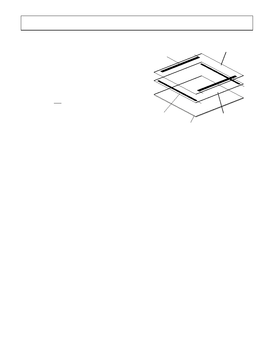
TOUCH SCREEN PRINCIPLES
A 4-wire touch screen consists of two flexible, transparent,
resistive-coated layers that are normally separated by a small
air gap (see Figure 22). The X layer has conductive electrodes
running down the left and right edges, allowing the application
of an excitation voltage across the X layer from left to right.
07667-
022
X+
X–
Y–
Y+
CONDUCTIVE ELECTRODE
ON BOTTOM SIDE
PLASTIC FILM WITH
TRANSPARENT, RESISTIVE
COATING ON BOTTOM SIDE
PLASTIC FILM WITH
TRANSPARENT, RESISTIVE
COATING ON TOP SIDE
LCD SCREEN
CONDUCTIVE ELECTRODE
ON TOP SIDE
Figure 22. Basic Construction of a Touch Screen
The Y layer has conductive electrodes running along the top
and bottom edges, allowing the application of an excitation
voltage down the Y layer from top to bottom.
Provided that the layers are of uniform resistivity, the voltage
at any point between the two electrodes is proportional to the
horizontal position for the X layer and the vertical position for
the Y layer.
When the screen is touched, the two layers make contact. If
only the X layer is excited, the voltage at the point of contact
and, therefore, the horizontal position, can be sensed at one of
the Y layer electrodes. Similarly, if only the Y layer is excited,
the voltage and, therefore, the vertical position, can be sensed
at one of the X layer electrodes. By switching alternately
between X and Y excitation and measuring the voltages, the
X and Y coordinates of the contact point can be determined.
In addition to measuring the X and Y coordinates, it is also
possible to estimate the touch pressure by measuring the
contact resistance between the X and Y layers. The AD7879/
AD7889 are designed to facilitate this measurement.
相关PDF资料 |
PDF描述 |
|---|---|
| AD7889-1ACBZ-RL | IC ADC 12BIT CTRLR TOUCH 12WLCSP |
| VE-BTV-IV-B1 | CONVERTER MOD DC/DC 5.8V 150W |
| VE-BT0-IV-B1 | CONVERTER MOD DC/DC 5V 150W |
| VE-B4H-IV-B1 | CONVERTER MOD DC/DC 52V 150W |
| AD7879-1ACPZ-RL | IC ADC 12BIT CTLR TOUCH 16LFCSP |
相关代理商/技术参数 |
参数描述 |
|---|---|
| AD7890ACHIPS-2 | 功能描述:Data Acquisition System (DAS) 12 bit 117k SPI Die 制造商:analog devices inc. 系列:- 包装:管件 零件状态:上次购买时间 类型:数据采集系统(DAS) 分辨率(位):12 b 采样率(每秒):117k 数据接口:SPI 电压源:单电源 电压 - 电源:5V 工作温度:-40°C ~ 85°C 安装类型:表面贴装 封装/外壳:模具 供应商器件封装:模具 标准包装:1 |
| AD7890AN-10 | 功能描述:IC DAS 12BIT 8CH 24-DIP RoHS:否 类别:集成电路 (IC) >> 数据采集 - ADCs/DAC - 专用型 系列:- 产品培训模块:Lead (SnPb) Finish for COTS Obsolescence Mitigation Program 标准包装:50 系列:- 类型:数据采集系统(DAS) 分辨率(位):16 b 采样率(每秒):21.94k 数据接口:MICROWIRE?,QSPI?,串行,SPI? 电压电源:模拟和数字 电源电压:1.8 V ~ 3.6 V 工作温度:-40°C ~ 85°C 安装类型:表面贴装 封装/外壳:40-WFQFN 裸露焊盘 供应商设备封装:40-TQFN-EP(6x6) 包装:托盘 |
| AD7890AN-2 | 功能描述:IC DAS 12BIT 8CH 24-DIP RoHS:否 类别:集成电路 (IC) >> 数据采集 - ADCs/DAC - 专用型 系列:- 产品培训模块:Lead (SnPb) Finish for COTS Obsolescence Mitigation Program 标准包装:50 系列:- 类型:数据采集系统(DAS) 分辨率(位):16 b 采样率(每秒):21.94k 数据接口:MICROWIRE?,QSPI?,串行,SPI? 电压电源:模拟和数字 电源电压:1.8 V ~ 3.6 V 工作温度:-40°C ~ 85°C 安装类型:表面贴装 封装/外壳:40-WFQFN 裸露焊盘 供应商设备封装:40-TQFN-EP(6x6) 包装:托盘 |
| AD7890AN-4 | 制造商:Analog Devices 功能描述:ADC Single SAR 117ksps 12-bit Serial 24-Pin PDIP 制造商:Rochester Electronics LLC 功能描述:8 CHANNEL,SERIAL A/D IC - Bulk |
| AD7890ANZ-10 | 功能描述:IC DAS 12BIT 8CH 24-DIP RoHS:是 类别:集成电路 (IC) >> 数据采集 - ADCs/DAC - 专用型 系列:- 产品培训模块:Lead (SnPb) Finish for COTS Obsolescence Mitigation Program 标准包装:50 系列:- 类型:数据采集系统(DAS) 分辨率(位):16 b 采样率(每秒):21.94k 数据接口:MICROWIRE?,QSPI?,串行,SPI? 电压电源:模拟和数字 电源电压:1.8 V ~ 3.6 V 工作温度:-40°C ~ 85°C 安装类型:表面贴装 封装/外壳:40-WFQFN 裸露焊盘 供应商设备封装:40-TQFN-EP(6x6) 包装:托盘 |
发布紧急采购,3分钟左右您将得到回复。