- 您现在的位置:买卖IC网 > PDF目录9713 > AD7889ACBZ-RL (Analog Devices Inc)IC ADC 12BIT CTRLR TOUCH 12WLCSP PDF资料下载
参数资料
| 型号: | AD7889ACBZ-RL |
| 厂商: | Analog Devices Inc |
| 文件页数: | 29/41页 |
| 文件大小: | 0K |
| 描述: | IC ADC 12BIT CTRLR TOUCH 12WLCSP |
| 产品变化通告: | 8mm Carrier Tape Changes 28/Feb/2012 |
| 标准包装: | 10,000 |
| 类型: | 电阻 |
| 触摸面板接口: | 4 线 |
| 输入数/键: | 1 TSC |
| 分辨率(位): | 12 b |
| 数据接口: | 串行,SPI? |
| 数据速率/采样率 (SPS,BPS): | 105k |
| 电压基准: | 外部 |
| 电源电压: | 1.6 V ~ 3.6 V |
| 电流 - 电源: | 10nA |
| 工作温度: | -40°C ~ 85°C |
| 安装类型: | 表面贴装 |
| 封装/外壳: | 12-UFBGA,WLCSP |
| 供应商设备封装: | 12-WLCSP |
| 包装: | 带卷 (TR) |
第1页第2页第3页第4页第5页第6页第7页第8页第9页第10页第11页第12页第13页第14页第15页第16页第17页第18页第19页第20页第21页第22页第23页第24页第25页第26页第27页第28页当前第29页第30页第31页第32页第33页第34页第35页第36页第37页第38页第39页第40页第41页
AD7879/AD7889
Rev. C | Page 34 of 40
07667-
041
DIN
CW
15
CW
14
CW
13
CW
8
CW
1
CW
0
X
SCL
CW
12
X
READBACK DATA FOR
STARTING REGISTER
ADDRESS
X
1
32
2
3
4
15
16
17
18
31
34
33
48
47
49
CS
CW
11
CW
10
CW
9
CW
7
CW
2
CW
6
CW
5
CW
4
CW
3
11
12
13
14
5
6
7
8
9
10
XXX
D15
D14
D1
D0
D1
D0
D15
D14
XXX
XXX XXX
XXX
XXX XXX
XXX
DOUT
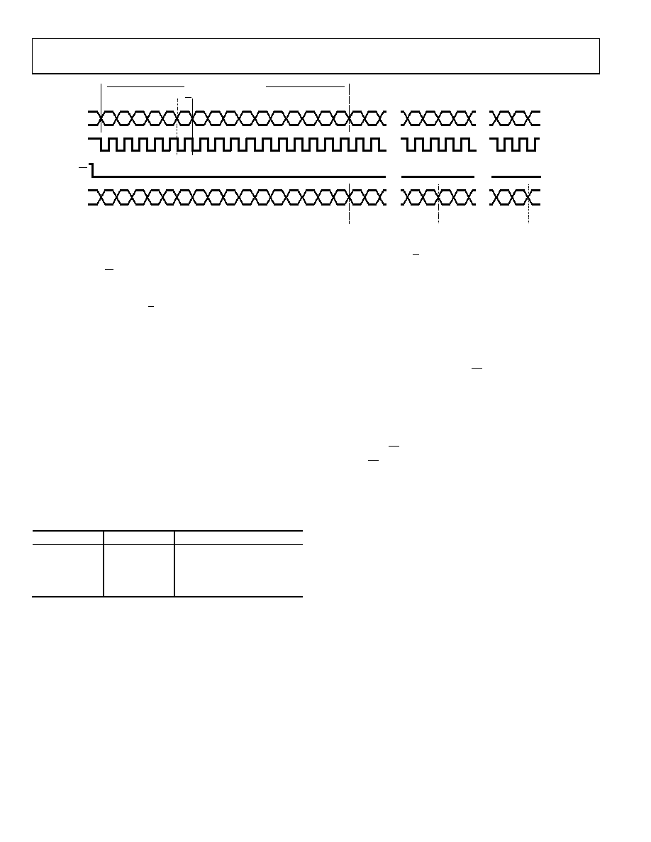
16-BIT COMMAND WORD
ENABLE WORD
R/W
STARTING REGISTER ADDRESS
NOTES
1. MULTIPLE SEQUENTIAL REGISTERS CAN BE READ BACK CONTINUOUSLY.
2. THE 16-BIT COMMAND WORD MUST BE WRITTEN ON DIN: 5 BITS FOR ENABLE WORD, 1 BIT FOR R/W, AND 10 BITS FOR REGISTER ADDRESS.
3. THE ADDRESS AUTOMATICALLY INCREMENTS WITH EACH 16-BIT DATA-WORD BEING READ BACK ON THE DOUT PIN.
4. CS IS HELD LOW UNTIL ALL REGISTER BITS HAVE BEEN READ BACK.
5. X DENOTES DON’T CARE.
6. XXX DENOTES HIGH IMPEDANCE THREE-STATE OUTPUT.
7. 16-BIT COMMAND WORD SETTINGS FOR SEQUENTIAL READBACK OPERATION:
CW[15:11] = 11100 (ENABLE WORD)
CW[10] = 1 (R/W)
CW[9:0] = [AD9, AD8, AD7, AD6, AD5, AD4, AD3, AD2, AD1, AD0] (STARTING MSB JUSTIFIED REGISTER ADDRESS)
READBACK DATA FOR
NEXT REGISTER ADDRESS
Figure 42. Sequential Register Readback, SPI Timing
I2C-COMPATIBLE INTERFACE
The AD7879-1/AD7889-1 support the industry standard 2-wire
I2C serial interface protocol. The two wires associated with the
I2C timing are the SCL and SDA inputs. SDA is an I/O pin that
allows both register write and register readback operations. The
AD7879-1/AD7889-1 are always slave devices on the I2C serial
interface bus.
The devices have a 7-bit device address, Address 0101 1XX. The
lower two bits are set by tying the ADD0 and ADD1 pins high or
low. The AD7879-1/AD7889-1 respond when the master device
sends its device address over the bus. The AD7879-1/AD7889-1
cannot initiate data transfers on the bus.
Table 25. I2C Device Addresses for the AD7879-1/AD7889-1
ADD1
ADD0
I2C Address
0
0101 100
0
1
0101 101
1
0
0101 110
1
0101 111
Data Transfer
Data is transferred over the I2C serial interface in 8-bit bytes.
The master initiates a data transfer by establishing a start
condition, defined as a high-to-low transition on the serial data
line, SDA, while the serial clock line, SCL, remains high. This
indicates that an address/data stream follows.
All slave peripherals connected to the serial bus respond to the
start condition and shift in the next eight bits, consisting of a
7-bit address (MSB first) plus a R/W bit that determines the
direction of the data transfer. The peripheral whose address
corresponds to the transmitted address responds by pulling the
data line low during the ninth clock pulse. This is known as the
acknowledge bit. All other devices on the bus then remain idle
while the selected device waits for data to be read from or written
to it. If the R/W bit is a 0, the master writes to the slave device.
If the R/W bit is a 1, the master reads from the slave device.
Data is sent over the serial bus in a sequence of nine clock
pulses (eight bits of data followed by an acknowledge bit from
the slave device). Transitions on the data line must occur during
the low period of the clock signal and remain stable during the
high period because a low-to-high transition when the clock
is high can be interpreted as a stop signal. The number of data
bytes transmitted over the serial bus in a single read or write
operation is limited only by what the master and slave devices
can handle.
When all data bytes are read or written, a stop condition is
established. A stop condition is defined by a low-to-high
transition on SDA while SCL remains high. If the AD7879-1/
AD7889-1 encounter a stop condition, they return to the idle
condition.
相关PDF资料 |
PDF描述 |
|---|---|
| AD7889-1ACBZ-RL | IC ADC 12BIT CTRLR TOUCH 12WLCSP |
| VE-BTV-IV-B1 | CONVERTER MOD DC/DC 5.8V 150W |
| VE-BT0-IV-B1 | CONVERTER MOD DC/DC 5V 150W |
| VE-B4H-IV-B1 | CONVERTER MOD DC/DC 52V 150W |
| AD7879-1ACPZ-RL | IC ADC 12BIT CTLR TOUCH 16LFCSP |
相关代理商/技术参数 |
参数描述 |
|---|---|
| AD7890ACHIPS-2 | 功能描述:Data Acquisition System (DAS) 12 bit 117k SPI Die 制造商:analog devices inc. 系列:- 包装:管件 零件状态:上次购买时间 类型:数据采集系统(DAS) 分辨率(位):12 b 采样率(每秒):117k 数据接口:SPI 电压源:单电源 电压 - 电源:5V 工作温度:-40°C ~ 85°C 安装类型:表面贴装 封装/外壳:模具 供应商器件封装:模具 标准包装:1 |
| AD7890AN-10 | 功能描述:IC DAS 12BIT 8CH 24-DIP RoHS:否 类别:集成电路 (IC) >> 数据采集 - ADCs/DAC - 专用型 系列:- 产品培训模块:Lead (SnPb) Finish for COTS Obsolescence Mitigation Program 标准包装:50 系列:- 类型:数据采集系统(DAS) 分辨率(位):16 b 采样率(每秒):21.94k 数据接口:MICROWIRE?,QSPI?,串行,SPI? 电压电源:模拟和数字 电源电压:1.8 V ~ 3.6 V 工作温度:-40°C ~ 85°C 安装类型:表面贴装 封装/外壳:40-WFQFN 裸露焊盘 供应商设备封装:40-TQFN-EP(6x6) 包装:托盘 |
| AD7890AN-2 | 功能描述:IC DAS 12BIT 8CH 24-DIP RoHS:否 类别:集成电路 (IC) >> 数据采集 - ADCs/DAC - 专用型 系列:- 产品培训模块:Lead (SnPb) Finish for COTS Obsolescence Mitigation Program 标准包装:50 系列:- 类型:数据采集系统(DAS) 分辨率(位):16 b 采样率(每秒):21.94k 数据接口:MICROWIRE?,QSPI?,串行,SPI? 电压电源:模拟和数字 电源电压:1.8 V ~ 3.6 V 工作温度:-40°C ~ 85°C 安装类型:表面贴装 封装/外壳:40-WFQFN 裸露焊盘 供应商设备封装:40-TQFN-EP(6x6) 包装:托盘 |
| AD7890AN-4 | 制造商:Analog Devices 功能描述:ADC Single SAR 117ksps 12-bit Serial 24-Pin PDIP 制造商:Rochester Electronics LLC 功能描述:8 CHANNEL,SERIAL A/D IC - Bulk |
| AD7890ANZ-10 | 功能描述:IC DAS 12BIT 8CH 24-DIP RoHS:是 类别:集成电路 (IC) >> 数据采集 - ADCs/DAC - 专用型 系列:- 产品培训模块:Lead (SnPb) Finish for COTS Obsolescence Mitigation Program 标准包装:50 系列:- 类型:数据采集系统(DAS) 分辨率(位):16 b 采样率(每秒):21.94k 数据接口:MICROWIRE?,QSPI?,串行,SPI? 电压电源:模拟和数字 电源电压:1.8 V ~ 3.6 V 工作温度:-40°C ~ 85°C 安装类型:表面贴装 封装/外壳:40-WFQFN 裸露焊盘 供应商设备封装:40-TQFN-EP(6x6) 包装:托盘 |
发布紧急采购,3分钟左右您将得到回复。