参数资料
| 型号: | AD7891ASZ-1 |
| 厂商: | Analog Devices Inc |
| 文件页数: | 10/20页 |
| 文件大小: | 0K |
| 描述: | IC DAS 12BIT 8CH HI-SPD 44-MQFP |
| 标准包装: | 1 |
| 类型: | 数据采集系统(DAS) |
| 分辨率(位): | 12 b |
| 采样率(每秒): | 500k |
| 数据接口: | 串行,并联 |
| 电压电源: | 单电源 |
| 电源电压: | 5V |
| 工作温度: | -40°C ~ 85°C |
| 安装类型: | 表面贴装 |
| 封装/外壳: | 44-QFP |
| 供应商设备封装: | 44-MQFP(10x10) |
| 包装: | 托盘 |
| 产品目录页面: | 776 (CN2011-ZH PDF) |
AD7891
–18–
REV. D
AD7891 PERFORMANCE
Linearity
The linearity of the AD7891 is primarily determined by the
on-chip 12-bit DAC. This is a segmented DAC that is laser
trimmed for 12-bit integral linearity and differential linearity.
Typical INL for the AD7891 is
±0.25 LSB while typical DNL
is
±0.5 LSB.
Noise
In an ADC, noise exhibits itself as code uncertainty in dc appli-
cations and as the noise floor (in an FFT for example) in ac
applications. In a sampling ADC, such as the AD7891, all
information about the analog input appears in the baseband from
dc to half the sampling frequency. The input bandwidth of the
track/hold amplifier exceeds the Nyquist bandwidth and,
therefore, an antialiasing filter should be used to remove
unwanted signals above fS/2 in the input signal in applications
where such signals exist.
Figure 17 shows a histogram plot for 16384 conversions of a dc
input signal using the AD7891-1. The analog input was set at
the center of a code transition in the following way. An initial dc
input level was selected and a number of conversions were
made. The resulting histogram was noted and the applied level
was adjusted so that only two codes were generated with an
equal number of occurrences. This indicated that the transition
point between the two codes had been found. The voltage level
at which this occurred was recorded. The other edge of one of
these two codes was then found in a similar manner. The dc
level for the center of code could then be calculated as the
average of the two transition levels. The AD7891-1 inputs
were configured for the
±5 V input range and the data was read
from the part in parallel mode after conversion. Similar results
have been found with the AD7891-1 on the
±10 V range and on
all input ranges of the AD7891-2. The same performance is
achieved in serial mode, again with the data read from the
AD7891-1 after conversion. All the codes, except for 3, appear
in one output bin, indicating excellent noise performance from
the ADC.
OUTPUT CODE
18000
16000
0
2148
2149
NUMBER
OF
OCCURRENCES
2150
8000
6000
4000
2000
12000
10000
14000
16381 CODES
1 CODE
2 CODES
Figure 17. Typical Histogram Plot (AD7891-1)
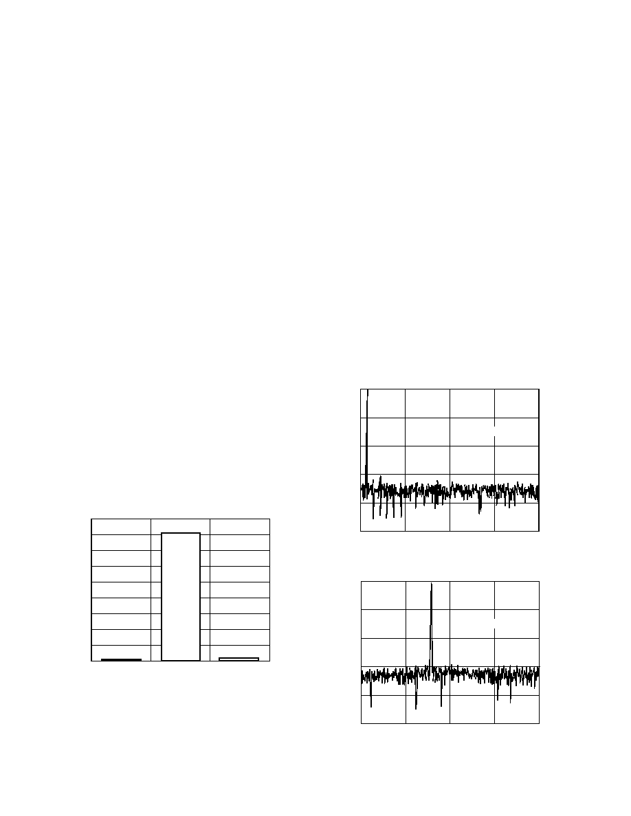
Dynamic Performance
The AD7891 contains an on-chip track/hold amplifier, allowing
the part to sample input signals of up to 250 kHz on any of its
input channels. Many of the AD7891’s applications require it to
sequence through low frequency input signals across its eight
channels. There may be some applications, however, for which
the dynamic performance of the converter on signals of up to
250 kHz input frequency is of interest. It is recommended for
these wider bandwidth signals that the hardware conversion
start method of sampling is used.
These applications require information on the spectral content
of the input signal. Signal-to-(noise + distortion), total
harmonic distortion, peak harmonic or spurious tone, and
intermodulation distortion are all specified. Figure 18 shows a
typical FFT plot of a 10 kHz,
±10 V input after being digitized
by the AD7891-1 operating at 500 kHz, with the input connected
for
±10 V operation. The signal-to-(noise + distortion) ratio is
72.2 dB and the total harmonic distortion is –87 dB. Figure 19
shows a typical FFT plot of a 100 kHz, 0 V to 5 V input after
being digitized by the AD7891-2 operating at 500 kHz, with the
input connected for 0 V to 5 V operation. The signal-to-(noise +
distortion) ratio is 71.17 dB and the total harmonic distortion
is –82.3 dB. It should be noted that reading from the part
during conversion does have a significant impact on dynamic
performance. Therefore, for sampling applications, it is
recommended not to read during conversion.
0
–30
–150
dB
–60
–90
–120
FS/2
2048 POINT FFT
SNR = 72.2dB
Figure 18. Typical AD7891-1 FFT Plot
0
–30
–150
dB
–60
–90
–120
FS/2
2048 POINT FFT
SNR = 71.17dB
Figure 19. Typical AD7891-2 FFT Plot
相关PDF资料 |
PDF描述 |
|---|---|
| VE-2TL-MY-S | CONVERTER MOD DC/DC 28V 50W |
| NC7SZ384P5X | IC BUS SWITCH 1BIT LP SC70-5 |
| D38999/26JJ61JA | CONN PLUG 61POS STRAIGHT W/SCKT |
| VE-B54-IU-S | CONVERTER MOD DC/DC 48V 200W |
| VE-2TH-MY-S | CONVERTER MOD DC/DC 52V 50W |
相关代理商/技术参数 |
参数描述 |
|---|---|
| AD7891ASZ-1 | 制造商:Analog Devices 功能描述:IC 12-BIT ADC |
| AD7891ASZ-1REEL | 功能描述:IC DAS 12BIT 8CH 44-MQFP RoHS:是 类别:集成电路 (IC) >> 数据采集 - ADCs/DAC - 专用型 系列:- 产品培训模块:Lead (SnPb) Finish for COTS Obsolescence Mitigation Program 标准包装:50 系列:- 类型:数据采集系统(DAS) 分辨率(位):16 b 采样率(每秒):21.94k 数据接口:MICROWIRE?,QSPI?,串行,SPI? 电压电源:模拟和数字 电源电压:1.8 V ~ 3.6 V 工作温度:-40°C ~ 85°C 安装类型:表面贴装 封装/外壳:40-WFQFN 裸露焊盘 供应商设备封装:40-TQFN-EP(6x6) 包装:托盘 |
| AD7891ASZ-2 | 功能描述:IC DAS 12BIT 8CH 44-MQFP RoHS:是 类别:集成电路 (IC) >> 数据采集 - ADCs/DAC - 专用型 系列:- 产品培训模块:Lead (SnPb) Finish for COTS Obsolescence Mitigation Program 标准包装:50 系列:- 类型:数据采集系统(DAS) 分辨率(位):16 b 采样率(每秒):21.94k 数据接口:MICROWIRE?,QSPI?,串行,SPI? 电压电源:模拟和数字 电源电压:1.8 V ~ 3.6 V 工作温度:-40°C ~ 85°C 安装类型:表面贴装 封装/外壳:40-WFQFN 裸露焊盘 供应商设备封装:40-TQFN-EP(6x6) 包装:托盘 |
| AD7891ASZ-2REEL | 功能描述:IC DAS 12BIT 8CH 44-MQFP RoHS:是 类别:集成电路 (IC) >> 数据采集 - ADCs/DAC - 专用型 系列:- 产品培训模块:Lead (SnPb) Finish for COTS Obsolescence Mitigation Program 标准包装:50 系列:- 类型:数据采集系统(DAS) 分辨率(位):16 b 采样率(每秒):21.94k 数据接口:MICROWIRE?,QSPI?,串行,SPI? 电压电源:模拟和数字 电源电压:1.8 V ~ 3.6 V 工作温度:-40°C ~ 85°C 安装类型:表面贴装 封装/外壳:40-WFQFN 裸露焊盘 供应商设备封装:40-TQFN-EP(6x6) 包装:托盘 |
| AD7891BP1 | 制造商:Analog Devices 功能描述: |
发布紧急采购,3分钟左右您将得到回复。