参数资料
| 型号: | AD7891ASZ-1 |
| 厂商: | Analog Devices Inc |
| 文件页数: | 8/20页 |
| 文件大小: | 0K |
| 描述: | IC DAS 12BIT 8CH HI-SPD 44-MQFP |
| 标准包装: | 1 |
| 类型: | 数据采集系统(DAS) |
| 分辨率(位): | 12 b |
| 采样率(每秒): | 500k |
| 数据接口: | 串行,并联 |
| 电压电源: | 单电源 |
| 电源电压: | 5V |
| 工作温度: | -40°C ~ 85°C |
| 安装类型: | 表面贴装 |
| 封装/外壳: | 44-QFP |
| 供应商设备封装: | 44-MQFP(10x10) |
| 包装: | 托盘 |
| 产品目录页面: | 776 (CN2011-ZH PDF) |
AD7891
–16–
REV. D
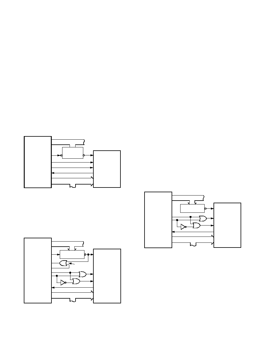
PARALLEL INTERFACING
The parallel port on the AD7891 allows the device to be interfaced
to microprocessors or DSP processors as a memory mapped
or I/O mapped device. The
CS and RD inputs are common to
all memory peripheral interfacing. Typical interfaces to different
processors are shown in Figures 12 to 15. In all the interfaces
shown, an external timer controls the
CONVST input of the
AD7891 and the
EOC output interrupts the host DSP.
AD7891 to ADSP-21xx
Figure 12 shows the AD7891 interfaced to the ADSP-21xx
series of DSPs as a memory mapped device. A single wait state
may be necessary to interface the AD7891 to the ADSP-21xx
depending on the clock speed of the DSP. This wait state can
be programmed via the data memory wait state control register
of the ADSP-21xx (please see the ADSP-2100 family Users
Manual for details). The following instruction reads data
from the AD7891.
MR = DM (ADC)
where ADC is the address of the AD7891.
DATA BUS
ADDRESS BUS
DB11 TO DB0
AD7891*
*ADDITIONAL PINS OMITTED FOR CLARITY
CS
WR
IRQ2
D23 TO D8
EOC
RD
WR
RD
ADDR
DECODE
EN
DMS
ADSP-21xx*
A13 TO A0
Figure 12. AD7891 to ADSP-21xx Parallel Interface
AD7891 to TMS32020, TMS320C25, and TMS320C5x
Parallel interfaces between the AD7891 and the TMS32020,
TMS320C25, and TMS320C5x family of DSPs are shown in
Figure 13. The memory mapped address chosen for the
AD7891 should be chosen to fall in the I/O memory space of
the DSPs.
TMS320C25
ONLY
DATA BUS
ADDRESS BUS
DB11 TO DB0
AD7891*
*ADDITIONAL PINS OMITTED FOR CLARITY
CS
WR
INTx
D23 TO D0
EOC
RD
MSC
ADDR
DECODE
EN
IS
A15 TO A0
TMS32020/
TMS320C25/
TMS320C5x*
READY
R/
W
STRB
Figure 13. AD7891 to TMS32020/TMS320C25/TMS320C5x
Parallel Interface
The parallel interface on the AD7891 is fast enough to interface
to the TMS32020 with no extra wait states. If high speed glue
logic, such as 74AS devices, are used to drive the
WR and RD
lines when interfacing to the TMS320C25, then again no wait
states are necessary. However, if slower logic is used, data accesses
may be slowed sufficiently when reading from and writing to the
part to require the insertion of one wait state. In such a case,
this wait state can be generated using the single OR gate to
combine the
CS and MSC signals to drive the READY line of
the TMS320C25, as shown in Figure 13. Extra wait states are
necessary when using the TMS320C5x at their fastest clock
speeds. Wait states can be programmed via the IOWSR and
CWSR registers (see the TMS320C5x User Guide for details).
Data is read from the ADC using the following instruction:
IN D, ADC
where D is the memory location where the data is to be stored,
and ADC is the I/O address of the AD7891.
AD7891 to TMS320C3x
Figure 14 shows a parallel interface between the AD7891 and
the TMS320C3x family of DSPs. The AD7891 is interfaced to
the expansion bus of the TMS320C3x. A single wait state is
required in this interface. This can be programmed using the
WTCNT bits of the expansion bus control register (see the
TMS320C3x Users Guide for details). Data from the AD7891
can be read using the following instruction:
LDI
ARn Rx
,
where ARn is an auxiliary register containing the lower 16 bits
of the address of the AD7891 in the TMS320C3x memory
space, and Rx is the register into which the ADC data is loaded.
EXPANSION DATA BUS
ADDRESS BUS
DB11 TO DB0
AD7891*
*ADDITIONAL PINS OMITTED FOR CLARITY
CS
WR
INTx
XD23 TO XD0
EOC
RD
ADDR
DECODE
XA15 TO XA0
XR/
W
IOSTRB
TMS320C3x*
Figure 14. AD7891 to TMS320C3x Parallel Interface
相关PDF资料 |
PDF描述 |
|---|---|
| VE-2TL-MY-S | CONVERTER MOD DC/DC 28V 50W |
| NC7SZ384P5X | IC BUS SWITCH 1BIT LP SC70-5 |
| D38999/26JJ61JA | CONN PLUG 61POS STRAIGHT W/SCKT |
| VE-B54-IU-S | CONVERTER MOD DC/DC 48V 200W |
| VE-2TH-MY-S | CONVERTER MOD DC/DC 52V 50W |
相关代理商/技术参数 |
参数描述 |
|---|---|
| AD7891ASZ-1 | 制造商:Analog Devices 功能描述:IC 12-BIT ADC |
| AD7891ASZ-1REEL | 功能描述:IC DAS 12BIT 8CH 44-MQFP RoHS:是 类别:集成电路 (IC) >> 数据采集 - ADCs/DAC - 专用型 系列:- 产品培训模块:Lead (SnPb) Finish for COTS Obsolescence Mitigation Program 标准包装:50 系列:- 类型:数据采集系统(DAS) 分辨率(位):16 b 采样率(每秒):21.94k 数据接口:MICROWIRE?,QSPI?,串行,SPI? 电压电源:模拟和数字 电源电压:1.8 V ~ 3.6 V 工作温度:-40°C ~ 85°C 安装类型:表面贴装 封装/外壳:40-WFQFN 裸露焊盘 供应商设备封装:40-TQFN-EP(6x6) 包装:托盘 |
| AD7891ASZ-2 | 功能描述:IC DAS 12BIT 8CH 44-MQFP RoHS:是 类别:集成电路 (IC) >> 数据采集 - ADCs/DAC - 专用型 系列:- 产品培训模块:Lead (SnPb) Finish for COTS Obsolescence Mitigation Program 标准包装:50 系列:- 类型:数据采集系统(DAS) 分辨率(位):16 b 采样率(每秒):21.94k 数据接口:MICROWIRE?,QSPI?,串行,SPI? 电压电源:模拟和数字 电源电压:1.8 V ~ 3.6 V 工作温度:-40°C ~ 85°C 安装类型:表面贴装 封装/外壳:40-WFQFN 裸露焊盘 供应商设备封装:40-TQFN-EP(6x6) 包装:托盘 |
| AD7891ASZ-2REEL | 功能描述:IC DAS 12BIT 8CH 44-MQFP RoHS:是 类别:集成电路 (IC) >> 数据采集 - ADCs/DAC - 专用型 系列:- 产品培训模块:Lead (SnPb) Finish for COTS Obsolescence Mitigation Program 标准包装:50 系列:- 类型:数据采集系统(DAS) 分辨率(位):16 b 采样率(每秒):21.94k 数据接口:MICROWIRE?,QSPI?,串行,SPI? 电压电源:模拟和数字 电源电压:1.8 V ~ 3.6 V 工作温度:-40°C ~ 85°C 安装类型:表面贴装 封装/外壳:40-WFQFN 裸露焊盘 供应商设备封装:40-TQFN-EP(6x6) 包装:托盘 |
| AD7891BP1 | 制造商:Analog Devices 功能描述: |
发布紧急采购,3分钟左右您将得到回复。