- 您现在的位置:买卖IC网 > PDF目录10664 > AD7894BRZ-10 (Analog Devices Inc)IC ADC 14BIT SRL T/H LP 8-SOIC PDF资料下载
参数资料
| 型号: | AD7894BRZ-10 |
| 厂商: | Analog Devices Inc |
| 文件页数: | 10/12页 |
| 文件大小: | 0K |
| 描述: | IC ADC 14BIT SRL T/H LP 8-SOIC |
| 标准包装: | 1 |
| 位数: | 14 |
| 采样率(每秒): | 200k |
| 数据接口: | 串行 |
| 转换器数目: | 1 |
| 功率耗散(最大): | 27.5mW |
| 电压电源: | 单电源 |
| 工作温度: | -40°C ~ 85°C |
| 安装类型: | 表面贴装 |
| 封装/外壳: | 8-SOIC(0.154",3.90mm 宽) |
| 供应商设备封装: | 8-SOIC |
| 包装: | 管件 |
| 输入数目和类型: | 1 个单端,双极 |
| 产品目录页面: | 779 (CN2011-ZH PDF) |
AD7894
–7–
REV. 0
Track/Hold Section
The track/hold amplifier on the analog input of the AD7894
allows the ADC to accurately convert an input sine wave of full-
scale amplitude to 14-bit accuracy. The input bandwidth of the
track/hold is greater than the Nyquist rate of the ADC, even
when the ADC is operated at its maximum throughput rate of
160 kHz (i.e., the track/hold can handle input frequencies in
excess of 100 kHz).
The track/hold amplifier acquires an input signal to 14-bit accu-
racy in less than 0.35
s. The operation of the track/hold is
essentially transparent to the user. With the high sampling
operating mode the track/hold amplifier goes from its tracking
mode to its hold mode at the start of conversion (i.e., the falling
edge of
CONVST). The aperture time for the track/hold (i.e.,
the delay time between the external
CONVST signal and the
track/hold actually going into hold) is typically 15 ns. At the
end of conversion (on the falling edge of BUSY) the part re-
turns to its tracking mode. The acquisition time of the track/
hold amplifier begins at this point. For the auto shutdown mode,
the rising edge of
CONVST wakes up the part and the track
and hold amplifier goes from its tracking mode to its hold mode
5
s after the rising edge of CONVST (provided that the
CONVST high time is less than 5
s). Once again the part re-
turns to its tracking mode at the end of conversion when the
BUSY signal goes low.
Reference Input
The reference input to the AD7894 is buffered on-chip with a
maximum reference input current of 1
A. The part is specified
with a +2.5 V reference input voltage. Errors in the reference
source will result in gain errors in the AD7894’s transfer func-
tion and will add to the specified full-scale errors on the part.
Suitable reference sources for the AD7894 include the AD780
and AD680 precision +2.5 V references.
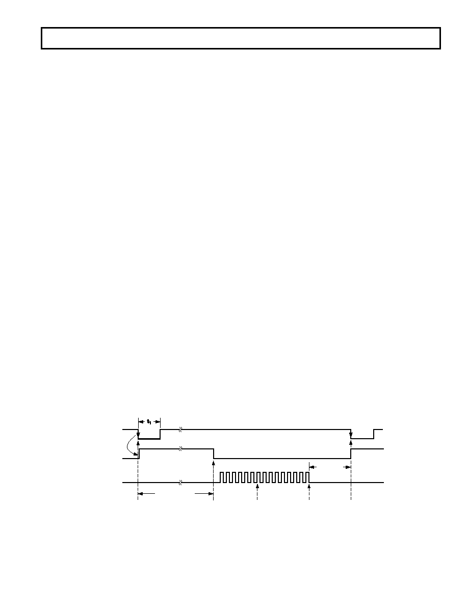
Timing and Control Section
Figure 3 shows the timing and control sequence required to
obtain optimum performance from the AD7894. In the se-
quence shown, conversion is initiated on the falling edge of
CONVST and new data from this conversion is available in the
output register of the AD7894 5
s later. Once the read opera-
tion has taken place, a further 250 ns should be allowed before
the next falling edge of
CONVST to optimize the settling of the
track/hold amplifier before the next conversion is initiated.
With the serial clock frequency at its maximum of 16 MHz, the
achievable throughput rate for the part is 5
s (conversion
time) plus 1.0
s (read time) plus 250 ns (quiet time). This
results in a minimum throughput time of 6.25
s (equivalent to
a throughput rate of 160 kHz). A serial clock of less than 16 MHz
can be used, but this will in turn mean that the throughput
time will increase.
The read operation consists of 16 serial clock pulses to the
output shift register of the AD7894. After 16 serial clock pulses
the shift register is reset and the SDATA line is three-stated. If
there are more serial clock pulses after the 16th clock, the shift
register will be moved on past its reset state. However, the shift
register will be reset again on the falling edge of the
CONVST
signal to ensure that the part returns to a known state every
conversion cycle. As a result, a read operation from the output
register should not straddle across the falling edge of
CONVST
as the output shift register will be reset in the middle of the
read operation and the data read back into the microprocessor
will appear invalid.
OPERATING MODES
Mode 1 Operation (High Sampling Performance)
The timing diagram in Figure 3 is for optimum performance in
operating Mode 1 where the falling edge of
CONVST starts
conversion and puts the Track/Hold amplifier into its hold
mode. This falling edge of
CONVST also causes the BUSY
signal to go high to indicate that a conversion is taking place.
The BUSY signal goes low when the conversion is complete,
which is 5
s max after the falling edge of CONVST and new
data from this conversion is available in the output register of
the AD7894. A read operation accesses this data. This read
operation consists of 16 clock cycles and the length of this read
operation will depend on the serial clock frequency. For the
fastest throughput rate (with a serial clock of 16 MHz) the read
operation will take 1.0
s. The read operation must be com-
plete at least 250 ns before the falling edge of the next
CONVST
and this gives a total time of 6.25
s for the full throughput
time (equivalent to 160 kHz). This mode of operation should
be used for high sampling applications.
250ns MIN
t1 = 40ns MIN
tCONVERT = 5 s
BUSY
SCLK
CONVST
CONVERSION IS
INITIATED;
TRACK/HOLD
GOES INTO HOLD
CONVERSION
ENDS
5 s LATER
SERIAL READ
OPERATION
READ OPERATION
SHOULD END
250ns PRIOR TO
NEXT FALLING
EDGE OF
CONVST
OUTPUT
SERIAL
SHIFT
REGISTER
IS RESET
Figure 3. Mode 1 Timing Operation Diagram for High Sampling Performance
相关PDF资料 |
PDF描述 |
|---|---|
| LMX393HAUA+T | IC COMPARATOR GP DUAL 8-UMAX |
| VI-B13-MX-F1 | CONVERTER MOD DC/DC 24V 75W |
| AD9214BRSZ-105 | IC ADC 10BIT 105MSPS 28-SSOP |
| AD7980BCPZ-RL7 | IC ADC 16BIT 1MSPS SAR 10LFCSP |
| VE-J1N-MW-F4 | CONVERTER MOD DC/DC 18.5V 100W |
相关代理商/技术参数 |
参数描述 |
|---|---|
| AD7894BRZ-10REEL | 功能描述:IC ADC 14BIT SRL T/H LP 8SOIC RoHS:是 类别:集成电路 (IC) >> 数据采集 - 模数转换器 系列:- 标准包装:1,000 系列:- 位数:12 采样率(每秒):300k 数据接口:并联 转换器数目:1 功率耗散(最大):75mW 电压电源:单电源 工作温度:0°C ~ 70°C 安装类型:表面贴装 封装/外壳:24-SOIC(0.295",7.50mm 宽) 供应商设备封装:24-SOIC 包装:带卷 (TR) 输入数目和类型:1 个单端,单极;1 个单端,双极 |
| AD7894BRZ-10REEL7 | 功能描述:IC ADC 14BIT SRL T/H LP 8SOIC RoHS:是 类别:集成电路 (IC) >> 数据采集 - 模数转换器 系列:- 标准包装:1,000 系列:- 位数:12 采样率(每秒):300k 数据接口:并联 转换器数目:1 功率耗散(最大):75mW 电压电源:单电源 工作温度:0°C ~ 70°C 安装类型:表面贴装 封装/外壳:24-SOIC(0.295",7.50mm 宽) 供应商设备封装:24-SOIC 包装:带卷 (TR) 输入数目和类型:1 个单端,单极;1 个单端,双极 |
| AD7894BRZ-3 | 功能描述:IC ADC 14BIT SRL T/H LP 8SOIC RoHS:是 类别:集成电路 (IC) >> 数据采集 - 模数转换器 系列:- 其它有关文件:TSA1204 View All Specifications 标准包装:1 系列:- 位数:12 采样率(每秒):20M 数据接口:并联 转换器数目:2 功率耗散(最大):155mW 电压电源:模拟和数字 工作温度:-40°C ~ 85°C 安装类型:表面贴装 封装/外壳:48-TQFP 供应商设备封装:48-TQFP(7x7) 包装:Digi-Reel® 输入数目和类型:4 个单端,单极;2 个差分,单极 产品目录页面:1156 (CN2011-ZH PDF) 其它名称:497-5435-6 |
| AD7895ACHIPS-10 | 功能描述:12 Bit Analog to Digital Converter 1 Input 1 SAR Die 制造商:analog devices inc. 系列:- 包装:托盘 - 晶粒 零件状态:上次购买时间 位数:12 采样率(每秒):192k 输入数:1 输入类型:单端 数据接口:SPI 配置:S/H-ADC 无线电 - S/H:ADC:1:1 A/D 转换器数:1 架构:SAR 参考类型:外部 电压 - 电源,模拟:5V 电压 - 电源,数字:5V 特性:- 工作温度:-40°C ~ 85°C 封装/外壳:模具 供应商器件封装:模具 标准包装:1 |
| AD7895AN-10 | 制造商:Analog Devices 功能描述:ADC Single SAR 192ksps 12-bit Serial 8-Pin PDIP 制造商:Rochester Electronics LLC 功能描述:- Bulk 制造商:Analog Devices 功能描述:IC 12-BIT ADC |
发布紧急采购,3分钟左右您将得到回复。