- 您现在的位置:买卖IC网 > PDF目录10664 > AD7894BRZ-10 (Analog Devices Inc)IC ADC 14BIT SRL T/H LP 8-SOIC PDF资料下载
参数资料
| 型号: | AD7894BRZ-10 |
| 厂商: | Analog Devices Inc |
| 文件页数: | 7/12页 |
| 文件大小: | 0K |
| 描述: | IC ADC 14BIT SRL T/H LP 8-SOIC |
| 标准包装: | 1 |
| 位数: | 14 |
| 采样率(每秒): | 200k |
| 数据接口: | 串行 |
| 转换器数目: | 1 |
| 功率耗散(最大): | 27.5mW |
| 电压电源: | 单电源 |
| 工作温度: | -40°C ~ 85°C |
| 安装类型: | 表面贴装 |
| 封装/外壳: | 8-SOIC(0.154",3.90mm 宽) |
| 供应商设备封装: | 8-SOIC |
| 包装: | 管件 |
| 输入数目和类型: | 1 个单端,双极 |
| 产品目录页面: | 779 (CN2011-ZH PDF) |
AD7894
–4–
REV. 0
ORDERING GUIDE
Temperature
Package
Model
Range
INL
Input Range
SNR
Description
Option
AD7894AR-10
–40
°C to +85°C
±2 LSB
±10 V
77 dB
8-Lead Narrow Body SOIC
SO-8
AD7894BR-10
–40
°C to +85°C
±1.5 LSB
±10 V
77 dB
8-Lead Narrow Body SOIC
SO-8
AD7894AR-3
–40
°C to +85°C
±2 LSB
±2.5 V
77 dB
8-Lead Narrow Body SOIC
SO-8
AD7894BR-3
–40
°C to +85°C
±1.5 LSB
±2.5 V
77 dB
8-Lead Narrow Body SOIC
SO-8
AD7894AR-2
–40
°C to +85°C
±2 LSB
0 V to +2.5 V
77 dB
8-Lead Narrow Body SOIC
SO-8
PIN FUNCTION DESCRIPTIONS
Pin
No.
Mnemonic
Description
1
REF IN
Voltage Reference Input. An external reference source should be connected to this pin to provide the
reference voltage for the AD7894’s conversion process. The REF IN input is buffered on-chip. The
nominal reference voltage for correct operation of the AD7894 is +2.5 V.
2VIN
Analog Input Channel. The analog input range is
±10 V (AD7894-10), ±2.5 V (AD7894-3) and 0 V to
+2.5 V (AD7894-2).
3
GND
Analog Ground. Ground reference for track/hold, comparator, digital circuitry and DAC.
4
SCLK
Serial Clock Input. An external serial clock is applied to this input to obtain serial data from the AD7894.
A new serial data bit is clocked out on the falling edge of this serial clock. Data is guaranteed valid for
10 ns after this falling edge so data can be accepted on the falling edge when a fast serial clock is used.
The serial clock input should be taken low at the end of the serial data transmission.
5
SDATA
Serial Data Output. Serial data from the AD7894 is provided at this output. The serial data is clocked
out by the falling edge of SCLK, but the data can also be read on the falling edge of SCLK. This is pos-
sible because data bit N is valid for a specified time after the falling edge of SCLK (data hold time) (see
Figure 5). Sixteen bits of serial data are provided as two leading zeroes followed by the 14 bits of conver-
sion data. On the 16th falling edge of SCLK, the SDATA line is held for the data hold time and then
disabled (three-stated). Output data coding is twos complement for the AD7894-10 and AD7894-3, and
straight binary for the AD7894-2.
6
BUSY
The BUSY pin is used to indicate when the part is doing a conversion. The BUSY pin will go high on
the falling edge of
CONVST and will return low when the conversion is complete.
7
CONVST
Conversion Start. Edge-triggered logic input. On the falling edge of this input, the track/hold goes into its
hold mode and conversion is initiated. If
CONVST is low at the end of conversion, the part goes into
power-down mode. In this case, the rising edge of
CONVST will cause the part to begin waking up.
8VDD
Positive supply voltage, +5 V
± 5%.
1.6mA
400 A
+1.6V
TO
OUTPUT
PIN
50pF
Figure 1. Load Circuit for Access Time and Bus
Relinquish Time
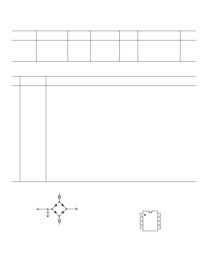
PIN CONFIGURATION
SOIC (SO-8)
TOP VIEW
(Not to Scale)
8
7
6
5
1
2
3
4
REF IN
VIN
GND
VDD
CONVST
BUSY
SDATA
SCLK
AD7894
相关PDF资料 |
PDF描述 |
|---|---|
| LMX393HAUA+T | IC COMPARATOR GP DUAL 8-UMAX |
| VI-B13-MX-F1 | CONVERTER MOD DC/DC 24V 75W |
| AD9214BRSZ-105 | IC ADC 10BIT 105MSPS 28-SSOP |
| AD7980BCPZ-RL7 | IC ADC 16BIT 1MSPS SAR 10LFCSP |
| VE-J1N-MW-F4 | CONVERTER MOD DC/DC 18.5V 100W |
相关代理商/技术参数 |
参数描述 |
|---|---|
| AD7894BRZ-10REEL | 功能描述:IC ADC 14BIT SRL T/H LP 8SOIC RoHS:是 类别:集成电路 (IC) >> 数据采集 - 模数转换器 系列:- 标准包装:1,000 系列:- 位数:12 采样率(每秒):300k 数据接口:并联 转换器数目:1 功率耗散(最大):75mW 电压电源:单电源 工作温度:0°C ~ 70°C 安装类型:表面贴装 封装/外壳:24-SOIC(0.295",7.50mm 宽) 供应商设备封装:24-SOIC 包装:带卷 (TR) 输入数目和类型:1 个单端,单极;1 个单端,双极 |
| AD7894BRZ-10REEL7 | 功能描述:IC ADC 14BIT SRL T/H LP 8SOIC RoHS:是 类别:集成电路 (IC) >> 数据采集 - 模数转换器 系列:- 标准包装:1,000 系列:- 位数:12 采样率(每秒):300k 数据接口:并联 转换器数目:1 功率耗散(最大):75mW 电压电源:单电源 工作温度:0°C ~ 70°C 安装类型:表面贴装 封装/外壳:24-SOIC(0.295",7.50mm 宽) 供应商设备封装:24-SOIC 包装:带卷 (TR) 输入数目和类型:1 个单端,单极;1 个单端,双极 |
| AD7894BRZ-3 | 功能描述:IC ADC 14BIT SRL T/H LP 8SOIC RoHS:是 类别:集成电路 (IC) >> 数据采集 - 模数转换器 系列:- 其它有关文件:TSA1204 View All Specifications 标准包装:1 系列:- 位数:12 采样率(每秒):20M 数据接口:并联 转换器数目:2 功率耗散(最大):155mW 电压电源:模拟和数字 工作温度:-40°C ~ 85°C 安装类型:表面贴装 封装/外壳:48-TQFP 供应商设备封装:48-TQFP(7x7) 包装:Digi-Reel® 输入数目和类型:4 个单端,单极;2 个差分,单极 产品目录页面:1156 (CN2011-ZH PDF) 其它名称:497-5435-6 |
| AD7895ACHIPS-10 | 功能描述:12 Bit Analog to Digital Converter 1 Input 1 SAR Die 制造商:analog devices inc. 系列:- 包装:托盘 - 晶粒 零件状态:上次购买时间 位数:12 采样率(每秒):192k 输入数:1 输入类型:单端 数据接口:SPI 配置:S/H-ADC 无线电 - S/H:ADC:1:1 A/D 转换器数:1 架构:SAR 参考类型:外部 电压 - 电源,模拟:5V 电压 - 电源,数字:5V 特性:- 工作温度:-40°C ~ 85°C 封装/外壳:模具 供应商器件封装:模具 标准包装:1 |
| AD7895AN-10 | 制造商:Analog Devices 功能描述:ADC Single SAR 192ksps 12-bit Serial 8-Pin PDIP 制造商:Rochester Electronics LLC 功能描述:- Bulk 制造商:Analog Devices 功能描述:IC 12-BIT ADC |
发布紧急采购,3分钟左右您将得到回复。