- 您现在的位置:买卖IC网 > PDF目录10577 > AD7910AKSZ-500RL7 (Analog Devices Inc)IC ADC 10BIT SRL 250KSPS SC70-6 PDF资料下载
参数资料
| 型号: | AD7910AKSZ-500RL7 |
| 厂商: | Analog Devices Inc |
| 文件页数: | 15/24页 |
| 文件大小: | 0K |
| 描述: | IC ADC 10BIT SRL 250KSPS SC70-6 |
| 标准包装: | 1 |
| 位数: | 10 |
| 采样率(每秒): | 250k |
| 数据接口: | DSP,MICROWIRE?,QSPI?,串行,SPI? |
| 转换器数目: | 1 |
| 功率耗散(最大): | 15mW |
| 电压电源: | 单电源 |
| 工作温度: | -40°C ~ 85°C |
| 安装类型: | 表面贴装 |
| 封装/外壳: | 6-TSSOP,SC-88,SOT-363 |
| 供应商设备封装: | SC-70-6 |
| 包装: | 标准包装 |
| 输入数目和类型: | 1 个单端,单极 |
| 其它名称: | AD7910AKSZ-500RL7DKR |
AD7910/AD7920
Rev. C | Page 22 of 24
APPLICATION HINTS
GROUNDING AND LAYOUT
The printed circuit board that houses the AD7910/AD7920
should be designed such that the analog and digital sections are
separated and confined to certain areas of the board. This
facilitates the use of ground planes that can be easily separated.
A minimum etch technique is generally best for ground planes
as it gives the best shielding. Digital and analog ground planes
should be joined at only one place. If the AD7910/AD7920 is in
a system where multiple devices require an AGND to DGND
connection then the connection should still be made at one
point only, a star ground point that should be established as
close to the AD7910/AD7920 as possible.
Avoid running digital lines under the device as these couple
noise onto the die. The analog ground plane should be allowed
to run under the AD7910/AD7920 to avoid noise coupling. The
power supply lines to the AD7910/AD7920 should use as large a
trace as possible to provide low impedance paths and reduce the
effects of glitches on the power supply line. Fast switching
signals like clocks should be shielded with digital ground to
avoid radiating noise to other sections of the board, and clock
signals should never be run near the analog inputs. Avoid
crossover of digital and analog signals. Traces on opposite sides
of the board should run at right angles to each other. This
reduces the effects of feedthrough through the board. A micro-
strip technique is by far the best but is not always possible with
a double-sided board. In this technique, the component side of
the board is dedicated to ground planes while signals are placed
on the solder side.
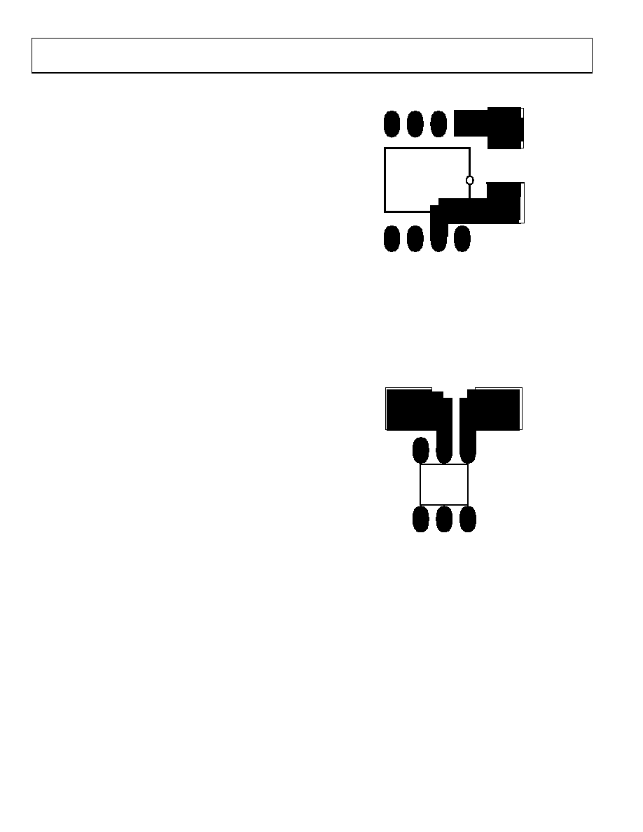
Good decoupling is also very important. The supply should be
decoupled with, for example, a 680 nF 0805 to GND. When
using the SC70 package in applications where the size of the
components is of concern, a 220 nF 0603 capacitor, for example,
could be used instead. However, in that case, the decoupling can
not be as effective and can result in an approximate SINAD
degradation of 0.3 dB. To achieve the best performance from
these decoupling components, the user should endeavor to keep
the distance between the decoupling capacitor and the VDD and
GND pins to a minimum with short track lengths connecting
recommended positions of the decoupling capacitor for the
MSOP and SC70 packages, respectively.
As can be seen in Figure 28, for the MSOP package, the
decoupling capacitor is placed as close as possible to the IC,
with short track lengths to VDD and GND pins. The decoupling
capacitor could also be placed on the underside of the PCB
directly underneath the IC, between the VDD and GND pins
attached by vias. This method would not be recommended on
PCBs above a standard 1.6 mm thickness. The best performance
is seen with the decoupling capacitor on the top of the PCB next
to the IC.
02976-028
Figure 28. Recommended Supply Decoupling Scheme for the
AD7910/AD7920 MSOP Package
Similarly, for the SC70 package, the decoupling capacitor should
be located as close as possible to the VDD and GND pins.
Because of its pinout, that is, VDD being next to GND, the
decoupling capacitor can be placed extremely close to the IC.
The decoupling capacitor could be placed on the underside of
the PCB directly under the VDD and GND pins, but, as before,
the best performance is seen with the decoupling capacitor on
the same side as the IC.
02976-029
Figure 29. Recommended Supply Decoupling Scheme for the
AD7910/AD7920 SC70 Package
EVALUATING PERFORMANCE
The evaluation board package includes a fully assembled and
tested evaluation board, documentation, and software for
controlling the board from the PC via the Eval-Board
Controller. To demonstrate/evaluate the ac and dc performance
of the AD7910/AD7920, the evaluation board controller can be
used in conjunction with the AD7910/AD7920CB evaluation
boards as well as many other Analog Devices’ evaluation boards
ending in the CB designator.
The software allows the user to perform ac (fast Fourier
transform) and dc (histogram of codes) tests on the
AD7910/AD7920. See the evaluation board technical note for
more information.
相关PDF资料 |
PDF描述 |
|---|---|
| MAX9132GUP+T | IC SW LVDS CROSSBAR 20TSSOP-EP |
| MAX11102ATB+T | IC ADC 12BIT SPI/SRL 10TDFN |
| 97-3106A-14S-6S | CONN PLUG 6POS W/SOCKETS |
| 97-3108B-14S-1P | CONN PLUG RT ANG 3POS W/PINS |
| MAX14886CTL+ | MUX DUAL HDMI LVL SHIFTER 40TQFN |
相关代理商/技术参数 |
参数描述 |
|---|---|
| AD7910AKSZ-REEL | 功能描述:IC ADC 10BIT SRL 250KSPS SC70-6 RoHS:是 类别:集成电路 (IC) >> 数据采集 - 模数转换器 系列:- 标准包装:2,500 系列:- 位数:16 采样率(每秒):15 数据接口:MICROWIRE?,串行,SPI? 转换器数目:1 功率耗散(最大):480µW 电压电源:单电源 工作温度:-40°C ~ 85°C 安装类型:表面贴装 封装/外壳:38-WFQFN 裸露焊盘 供应商设备封装:38-QFN(5x7) 包装:带卷 (TR) 输入数目和类型:16 个单端,双极;8 个差分,双极 配用:DC1011A-C-ND - BOARD DELTA SIGMA ADC LTC2494 |
| AD7910AKSZ-REEL7 | 功能描述:IC ADC 10BIT SRL 250KSPS SC70-6 RoHS:是 类别:集成电路 (IC) >> 数据采集 - 模数转换器 系列:- 标准包装:2,500 系列:- 位数:16 采样率(每秒):15 数据接口:MICROWIRE?,串行,SPI? 转换器数目:1 功率耗散(最大):480µW 电压电源:单电源 工作温度:-40°C ~ 85°C 安装类型:表面贴装 封装/外壳:38-WFQFN 裸露焊盘 供应商设备封装:38-QFN(5x7) 包装:带卷 (TR) 输入数目和类型:16 个单端,双极;8 个差分,双极 配用:DC1011A-C-ND - BOARD DELTA SIGMA ADC LTC2494 |
| AD7910ARM | 制造商:Analog Devices 功能描述:ADC Single SAR 250ksps 10-bit Serial 8-Pin MSOP 制造商:Analog Devices 功能描述:IC 10BIT ADC SMD 7910 MSOP8 |
| AD7910ARM-REEL | 制造商:Analog Devices 功能描述:ADC Single SAR 250ksps 10-bit Serial 8-Pin MSOP T/R 制造商:Analog Devices 功能描述:ADC SGL SAR 250KSPS 10-BIT SERL 8MSOP - Tape and Reel |
| AD7910ARM-REEL7 | 制造商:Analog Devices 功能描述:ADC Single SAR 250ksps 10-bit Serial 8-Pin MSOP T/R |
发布紧急采购,3分钟左右您将得到回复。