- 您现在的位置:买卖IC网 > PDF目录10577 > AD7910AKSZ-500RL7 (Analog Devices Inc)IC ADC 10BIT SRL 250KSPS SC70-6 PDF资料下载
参数资料
| 型号: | AD7910AKSZ-500RL7 |
| 厂商: | Analog Devices Inc |
| 文件页数: | 21/24页 |
| 文件大小: | 0K |
| 描述: | IC ADC 10BIT SRL 250KSPS SC70-6 |
| 标准包装: | 1 |
| 位数: | 10 |
| 采样率(每秒): | 250k |
| 数据接口: | DSP,MICROWIRE?,QSPI?,串行,SPI? |
| 转换器数目: | 1 |
| 功率耗散(最大): | 15mW |
| 电压电源: | 单电源 |
| 工作温度: | -40°C ~ 85°C |
| 安装类型: | 表面贴装 |
| 封装/外壳: | 6-TSSOP,SC-88,SOT-363 |
| 供应商设备封装: | SC-70-6 |
| 包装: | 标准包装 |
| 输入数目和类型: | 1 个单端,单极 |
| 其它名称: | AD7910AKSZ-500RL7DKR |
AD7910/AD7920
Rev. C | Page 6 of 24
TIMING SPECIFICATIONS
VDD = 2.35 V to 5.25 V, TA = TMIN to TMAX, unless otherwise noted.
Table 3.
Parameter1
AD7910/AD7920
Limit at TMIN, TMAX
Unit
Description
fSCLK2
10
kHz min3
5
MHz max
tCONVERT
14 × tSCLK
AD7910
16 × tSCLK
AD7920
tQUIET
50
ns min
Minimum quiet time required between bus relinquish and start of next
conversion
t1
10
ns min
Minimum CS pulse width
t2
10
ns min
CS to SCLK setup time
t34
22
ns max
Delay from CS until SDATA three-state disabled
t4
40
ns max
Data access time after SCLK falling edge
t5
0.4 × tSCLK
ns min
SCLK low pulse width
t6
0.4 × tSCLK
ns min
SCLK high pulse width
SCLK to data valid hold time
10
ns min
VDD ≤ 3.3 V
9.5
ns min
3.3 V < VDD ≤ 3.6 V
7
ns min
VDD > 3.6 V
t86, 7
36
ns max
SCLK falling edge to SDATA three-state
See Note 7
ns min
SCLK falling edge to SDATA three-state
tPOWER-UP8
1
μs max
Power-up time from full power-down
1 Guaranteed by characterization. All input signals are specified with tr = tf = 5 ns (10% to 90% of VDD) and timed from a voltage level of 1.6 V.
2 Mark/Space ratio for the SCLK input is 40/60 to 60/40.
3 Minimum fSCLK at which specifications are guaranteed.
4 Measured with the load circuit of Figure 2 and defined as the time required for the output to cross 0.8 V or 1.8 V when VDD = 2.35 V and 0.8 V or 2.0 V for VDD > 2.35 V.
5 Measured with a 50 pF load capacitor.
6 t8 is derived from the measured time taken by the data outputs to change 0.5 V when loaded with the circuit of Figure 2. The measured number is then extrapolated
back to remove the effects of charging or discharging the 50 pF capacitor. This means that the time, t8, shown in the Timing Specifications is the true bus relinquish
time of the part and is independent of the bus loading.
7 T7 values apply to t8 minimum values also.
8 See Power-Up Time section.
200
μAI
OL
200
μAI
OH
1.6V
TO OUTPUT
PIN
CL
50pF
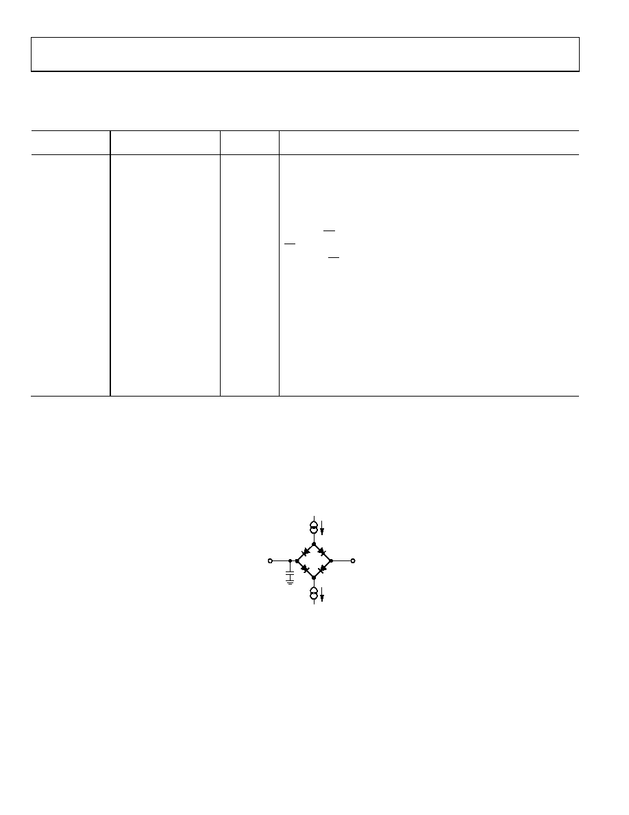
02976-002
Figure 2. Load Circuit for Digital Output Timing Specifications
相关PDF资料 |
PDF描述 |
|---|---|
| MAX9132GUP+T | IC SW LVDS CROSSBAR 20TSSOP-EP |
| MAX11102ATB+T | IC ADC 12BIT SPI/SRL 10TDFN |
| 97-3106A-14S-6S | CONN PLUG 6POS W/SOCKETS |
| 97-3108B-14S-1P | CONN PLUG RT ANG 3POS W/PINS |
| MAX14886CTL+ | MUX DUAL HDMI LVL SHIFTER 40TQFN |
相关代理商/技术参数 |
参数描述 |
|---|---|
| AD7910AKSZ-REEL | 功能描述:IC ADC 10BIT SRL 250KSPS SC70-6 RoHS:是 类别:集成电路 (IC) >> 数据采集 - 模数转换器 系列:- 标准包装:2,500 系列:- 位数:16 采样率(每秒):15 数据接口:MICROWIRE?,串行,SPI? 转换器数目:1 功率耗散(最大):480µW 电压电源:单电源 工作温度:-40°C ~ 85°C 安装类型:表面贴装 封装/外壳:38-WFQFN 裸露焊盘 供应商设备封装:38-QFN(5x7) 包装:带卷 (TR) 输入数目和类型:16 个单端,双极;8 个差分,双极 配用:DC1011A-C-ND - BOARD DELTA SIGMA ADC LTC2494 |
| AD7910AKSZ-REEL7 | 功能描述:IC ADC 10BIT SRL 250KSPS SC70-6 RoHS:是 类别:集成电路 (IC) >> 数据采集 - 模数转换器 系列:- 标准包装:2,500 系列:- 位数:16 采样率(每秒):15 数据接口:MICROWIRE?,串行,SPI? 转换器数目:1 功率耗散(最大):480µW 电压电源:单电源 工作温度:-40°C ~ 85°C 安装类型:表面贴装 封装/外壳:38-WFQFN 裸露焊盘 供应商设备封装:38-QFN(5x7) 包装:带卷 (TR) 输入数目和类型:16 个单端,双极;8 个差分,双极 配用:DC1011A-C-ND - BOARD DELTA SIGMA ADC LTC2494 |
| AD7910ARM | 制造商:Analog Devices 功能描述:ADC Single SAR 250ksps 10-bit Serial 8-Pin MSOP 制造商:Analog Devices 功能描述:IC 10BIT ADC SMD 7910 MSOP8 |
| AD7910ARM-REEL | 制造商:Analog Devices 功能描述:ADC Single SAR 250ksps 10-bit Serial 8-Pin MSOP T/R 制造商:Analog Devices 功能描述:ADC SGL SAR 250KSPS 10-BIT SERL 8MSOP - Tape and Reel |
| AD7910ARM-REEL7 | 制造商:Analog Devices 功能描述:ADC Single SAR 250ksps 10-bit Serial 8-Pin MSOP T/R |
发布紧急采购,3分钟左右您将得到回复。