参数资料
| 型号: | AD7927BRU |
| 厂商: | Analog Devices Inc |
| 文件页数: | 15/28页 |
| 文件大小: | 0K |
| 描述: | IC ADC 12BIT 8CH 200KSPS 20TSSOP |
| 标准包装: | 75 |
| 位数: | 12 |
| 采样率(每秒): | 200k |
| 数据接口: | DSP,MICROWIRE?,QSPI?,串行,SPI? |
| 转换器数目: | 1 |
| 功率耗散(最大): | 7.5mW |
| 电压电源: | 单电源 |
| 工作温度: | -40°C ~ 85°C |
| 安装类型: | 表面贴装 |
| 封装/外壳: | 20-TSSOP(0.173",4.40mm 宽) |
| 供应商设备封装: | 20-TSSOP |
| 包装: | 管件 |
| 输入数目和类型: | 8 个单端,单极 |
| 配用: | EVAL-AD7927CBZ-ND - BOARD EVALUATION FOR AD7927 |
第1页第2页第3页第4页第5页第6页第7页第8页第9页第10页第11页第12页第13页第14页当前第15页第16页第17页第18页第19页第20页第21页第22页第23页第24页第25页第26页第27页第28页
AD7927
Data Sheet
Rev. D | Page 22 of 28
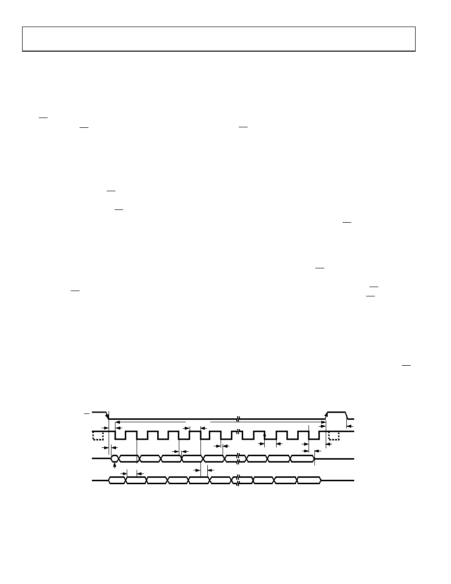
SERIAL INTERFACE
Figure 26 shows the detailed timing diagram for serial inter-
facing to the AD7927. The serial clock provides the conversion
clock and also controls the transfer of information to and from
the AD7927 during each conversion.
The CS signal initiates the data transfer and conversion process.
The falling edge of CS puts the track-and-hold into hold mode
and takes the bus out of three-state; the analog input is sampled
at this point. The conversion is also initiated at this point and
requires 16 SCLK cycles to complete. The track-and-hold goes
back into track on the 14th SCLK falling edge as shown in
Figure 26 at Point B, except when the write is to the shadow
register, in which case the track-and-hold does not return to
track until the rising edge of CS, that is, Point C in Figure 27.
On the 16th SCLK falling edge the DOUT line goes back into
three-state. If the rising edge of CS occurs before 16 SCLKs have
elapsed, the conversion is terminated and the DOUT line goes
back into three-state and the control register is not be updated;
otherwise DOUT returns to three-state on the 16th SCLK falling
edge, as shown in Figure 26. Sixteen serial clock cycles are
required to perform the conversion process and to access data
from the AD7927. For the AD7927, the 12 bits of data are
preceded by a leading zero and the three-channel address bits
(ADD2 to ADD0) identifying which channel the result
corresponds to. CS going low provides the leading zero to be
read in by the microcontroller or DSP. The three remaining
address bits and data bits are then clocked out by subsequent
SCLK falling edges beginning with the first address bit (ADD2)
thus the first falling clock edge on the serial clock has a leading
zero provided and also clocks out Address Bit ADD2. The final
bit in the data transfer is valid on the 16th falling edge, having
been clocked out on the previous (15th) falling edge.
Writing of information to the control register takes place on the
first 12 falling edges of SCLK in a data transfer, assuming the MSB
(that is, the WRITE bit) has been set to 1. If the control register
is programmed to use the shadow register, then the writing of
information to the shadow register takes place on all 16 SCLK
falling edges in the next serial transfer as shown for example on
the AD7927 in Figure 27. Two sequence options can be pro-
grammed in the shadow register. If the user does not want to
program a second sequence, then the eight LSBs should be filled
with zeros. The shadow register is updated upon the rising edge
of CS and the track-and-hold begins to track the first channel
selected in the sequence.
The 16-bit word read from the AD7927 always contains a leading
zero and three-channel address bits that the conversion result
corresponds to, followed by the 12-bit conversion result.
WRITING BETWEEN CONVERSIONS
As outlined in the Modes of Operation section, no less than 5 μs
should be left between consecutive valid conversions. However,
there is one case where this does not necessarily mean that at
least 5 μs should always be left between CS falling edges. Con-
sider the prior to a valid conversion. The user must write to the
part to tell it to power up before it can convert successfully. Once
the serial write to power up has finished, it may be desirable to
perform the conversion as soon as possible and not have to wait
a further 5 μs before bringing CS low for the conversion. In this
case, as long as there is a minimum of 5 μs between each valid
conversion, then only the quiet time between the CS rising edge
at the end of the write to power up and the next CS falling edge
for a valid conversion needs to be met (see Figure 28). Note that
when writing to the AD7927 between these valid conversions,
the DOUT line is not driven during the extra write operation,
as shown in Figure 28.
It is critical that an extra write operation as outlined previously
is never issued between valid conversions when the AD7927 is
executing through a sequence function, as the falling edge of CS
in the extra write would move the mux on to the next channel
in the sequence. This means when the next valid conversion
takes place, a channel result would have been missed.
SCLK
DOUT
DIN
B
ZERO
3 IDENTIFICATION BITS
WRITE
SEQ
DONTC
ADD2
ADD1
ADD0
DONTC
ADD2
ADD1
ADD0
DB11
DB10
DB2
DB1
DB0
THREE-STATE
tQUIET
16
15
14
13
5
4
3
2
1
THREE-
STATE
tCONVERT
CS
t2
t3
t9
t6
t4
t10
t7
t5
t8
t11
030
88
-0
26
Figure 26. Serial Interface Timing Diagram
相关PDF资料 |
PDF描述 |
|---|---|
| AD7934BRUZ | IC ADC 12BIT 4CH 1.5MSPS 28TSSOP |
| AD7938BCPZ-6 | IC ADC 12BIT 8CH 625KSPS 32LFCSP |
| AD7938BCPZ | IC ADC 12BIT 8CH 1.5MSPS 32LFCSP |
| AD7940BRM | IC ADC 14BIT UNIPOLAR 8-MSOP |
| AD7942BRMZ-RL7 | IC ADC 14BIT 250KSPS 10-MSOP |
相关代理商/技术参数 |
参数描述 |
|---|---|
| AD7927BRU-REEL | 制造商:Analog Devices 功能描述:ADC Single SAR 200ksps 12-bit Serial 20-Pin TSSOP T/R 制造商:Analog Devices 功能描述:ADC SGL SAR 200KSPS 12-BIT SERL 20TSSOP - Tape and Reel |
| AD7927BRU-REEL7 | 制造商:Analog Devices 功能描述:ADC Single SAR 200ksps 12-bit Serial 20-Pin TSSOP T/R |
| AD7927BRUZ | 功能描述:IC ADC 12BIT 8CH 200KSPS 20TSSOP RoHS:是 类别:集成电路 (IC) >> 数据采集 - 模数转换器 系列:- 标准包装:1 系列:microPOWER™ 位数:8 采样率(每秒):1M 数据接口:串行,SPI? 转换器数目:1 功率耗散(最大):- 电压电源:模拟和数字 工作温度:-40°C ~ 125°C 安装类型:表面贴装 封装/外壳:24-VFQFN 裸露焊盘 供应商设备封装:24-VQFN 裸露焊盘(4x4) 包装:Digi-Reel® 输入数目和类型:8 个单端,单极 产品目录页面:892 (CN2011-ZH PDF) 其它名称:296-25851-6 |
| AD7927BRUZ | 制造商:Analog Devices 功能描述:IC 12BIT ADC SMD 7927 TSSOP20 |
| AD7927BRUZ-REEL | 功能描述:IC ADC 12BIT 8CH W/SEQ 20TSSOP RoHS:是 类别:集成电路 (IC) >> 数据采集 - 模数转换器 系列:- 标准包装:2,500 系列:- 位数:16 采样率(每秒):15 数据接口:MICROWIRE?,串行,SPI? 转换器数目:1 功率耗散(最大):480µW 电压电源:单电源 工作温度:-40°C ~ 85°C 安装类型:表面贴装 封装/外壳:38-WFQFN 裸露焊盘 供应商设备封装:38-QFN(5x7) 包装:带卷 (TR) 输入数目和类型:16 个单端,双极;8 个差分,双极 配用:DC1011A-C-ND - BOARD DELTA SIGMA ADC LTC2494 |
发布紧急采购,3分钟左右您将得到回复。