- 您现在的位置:买卖IC网 > PDF目录1984 > AD7938BCPZ-6 (Analog Devices Inc)IC ADC 12BIT 8CH 625KSPS 32LFCSP PDF资料下载
参数资料
| 型号: | AD7938BCPZ-6 |
| 厂商: | Analog Devices Inc |
| 文件页数: | 18/32页 |
| 文件大小: | 0K |
| 描述: | IC ADC 12BIT 8CH 625KSPS 32LFCSP |
| 标准包装: | 1 |
| 位数: | 12 |
| 采样率(每秒): | 625k |
| 数据接口: | 并联 |
| 转换器数目: | 1 |
| 功率耗散(最大): | 7.5mW |
| 电压电源: | 单电源 |
| 工作温度: | -40°C ~ 85°C |
| 安装类型: | 表面贴装 |
| 封装/外壳: | 32-VFQFN 裸露焊盘,CSP |
| 供应商设备封装: | 32-LFCSP-VQ |
| 包装: | 托盘 |
| 输入数目和类型: | 8 个单端,单极;4 个差分,单极;4 个伪差分,单极;7 伪差分,单极 |
| 配用: | EVAL-AD7938CBZ-ND - EVAL BOARD FOR AD7938 |
第1页第2页第3页第4页第5页第6页第7页第8页第9页第10页第11页第12页第13页第14页第15页第16页第17页当前第18页第19页第20页第21页第22页第23页第24页第25页第26页第27页第28页第29页第30页第31页第32页
Data Sheet
AD7938-6
Rev. C | Page 25 of 32
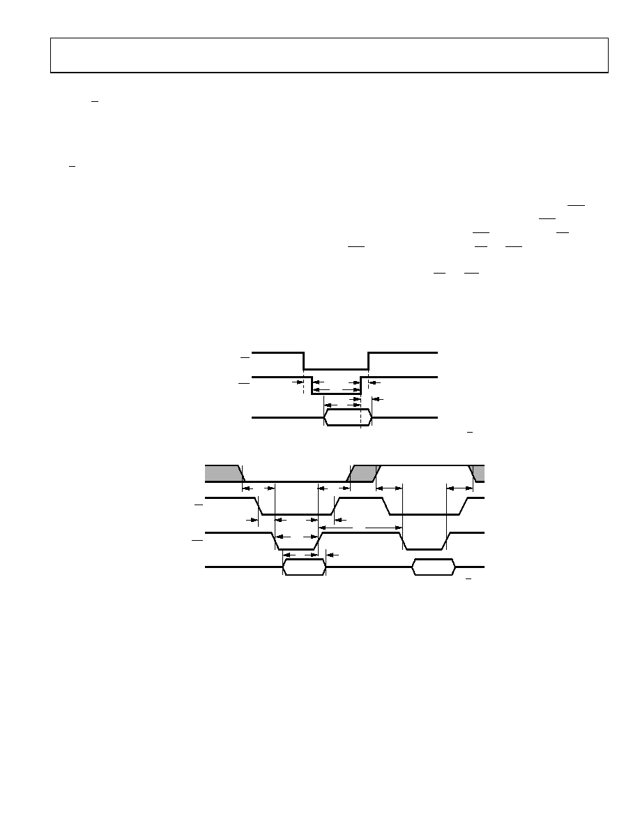
Writing Data to the AD7938-6
With W/B tied logic high, a single write operation transfers the
full data-word on DB0 to DB11 to the control register on the
AD7938-6. The DB8/HBEN pin assumes its DB8 function. Data
written to the AD7938-6 should be provided on the DB0 to
DB11 inputs with DB0 being the LSB of the data-word. With
W/B tied logic low, the AD7938-6 requires two write operations
to transfer a full 12-bit word. DB8/HBEN assumes its HBEN
function. Data written to the AD7938-6 should be provided on
the DB0 to DB7 inputs. HBEN determines whether the byte
written is high byte or low byte data. The low byte of the data-
word should be written first with DB0 being the LSB of the full
data-word. For the high byte write, HBEN should be high and
the data on the DB0 input should be Bit 8 of the 12-bit word. In
both word mode and byte mode, a single write operation to the
shadow register is always sufficient since it is only 8-bits wide.
Figure 37 shows the write cycle timing diagram of the AD7938-6
in word mode. When operating in word mode, the HBEN input
does not exist and only one write operation is required to write
the word of data to the device. Data should be provided on DB0
to DB11. When operating in byte mode, the two write cycles
shown in Figure 38 are required to write the full data-word to
the AD7938-6. In Figure 38, the first write transfers the lower
eight bits of the data-word from DB0 to DB7, and the second
write transfers the upper four bits of the data-word. When
writing to the AD7938-6, the top four bits in the high byte must
be 0s.
The data is latched into the device on the rising edge of WR.
The data needs to be set up a time, t7, before the WR rising edge
and held for a time, t8, after the WR rising edge. The CS and
WR signals are gated internally. CS and WR can be tied
together as the timing specifications for t4 and t5 are 0 ns
minimum (assuming CS and RD have not already been tied
together).
t8
t5
t7
t6
t4
DATA
DB0 TO DB11
WR
CS
04
75
1-
00
2
Figure 37. AD7938-6 Parallel Interface—Write Cycle Timing for Word Mode Operation (W/B = 1)
t5
t4
t7
t18
t19
t8
t6
t17
LOW BYTE
HIGH BYTE
DB0 TO DB11
HBEN/DB8
WR
CS
04
75
1-
0
03
Figure 38. AD7938-6 Parallel Interface—Write Cycle Timing for Byte Mode Operation (W/B = 0)
相关PDF资料 |
PDF描述 |
|---|---|
| AD7938BCPZ | IC ADC 12BIT 8CH 1.5MSPS 32LFCSP |
| AD7940BRM | IC ADC 14BIT UNIPOLAR 8-MSOP |
| AD7942BRMZ-RL7 | IC ADC 14BIT 250KSPS 10-MSOP |
| AD7944BCPZ | IC ADC 14BIT 2.5MSPS 20LFCSP |
| AD7946BCPZRL7 | IC ADC 14BIT 500KSPS 10-LFCSP |
相关代理商/技术参数 |
参数描述 |
|---|---|
| AD7938BCPZ-6REEL7 | 功能描述:IC ADC 12BIT 8CH 625KSPS 32LFCSP RoHS:是 类别:集成电路 (IC) >> 数据采集 - 模数转换器 系列:- 标准包装:1,000 系列:- 位数:16 采样率(每秒):45k 数据接口:串行 转换器数目:2 功率耗散(最大):315mW 电压电源:模拟和数字 工作温度:0°C ~ 70°C 安装类型:表面贴装 封装/外壳:28-SOIC(0.295",7.50mm 宽) 供应商设备封装:28-SOIC W 包装:带卷 (TR) 输入数目和类型:2 个单端,单极 |
| AD7938BCPZ-REEL7 | 功能描述:IC ADC 12BIT 8CH 1.5MSPS 32LFCSP RoHS:是 类别:集成电路 (IC) >> 数据采集 - 模数转换器 系列:- 标准包装:1,000 系列:- 位数:12 采样率(每秒):300k 数据接口:并联 转换器数目:1 功率耗散(最大):75mW 电压电源:单电源 工作温度:0°C ~ 70°C 安装类型:表面贴装 封装/外壳:24-SOIC(0.295",7.50mm 宽) 供应商设备封装:24-SOIC 包装:带卷 (TR) 输入数目和类型:1 个单端,单极;1 个单端,双极 |
| AD7938BSU | 制造商:Analog Devices 功能描述: |
| AD7938BSU-6 | 制造商:Analog Devices 功能描述:ADC Single SAR 625ksps 12-bit Parallel 32-Pin TQFP |
| AD7938BSU-6REEL | 制造商:AD 制造商全称:Analog Devices 功能描述:8-Channel, 625 kSPS, 12-Bit Parallel ADCs with a Sequencer |
发布紧急采购,3分钟左右您将得到回复。