- 您现在的位置:买卖IC网 > PDF目录1984 > AD7938BCPZ-6 (Analog Devices Inc)IC ADC 12BIT 8CH 625KSPS 32LFCSP PDF资料下载
参数资料
| 型号: | AD7938BCPZ-6 |
| 厂商: | Analog Devices Inc |
| 文件页数: | 5/32页 |
| 文件大小: | 0K |
| 描述: | IC ADC 12BIT 8CH 625KSPS 32LFCSP |
| 标准包装: | 1 |
| 位数: | 12 |
| 采样率(每秒): | 625k |
| 数据接口: | 并联 |
| 转换器数目: | 1 |
| 功率耗散(最大): | 7.5mW |
| 电压电源: | 单电源 |
| 工作温度: | -40°C ~ 85°C |
| 安装类型: | 表面贴装 |
| 封装/外壳: | 32-VFQFN 裸露焊盘,CSP |
| 供应商设备封装: | 32-LFCSP-VQ |
| 包装: | 托盘 |
| 输入数目和类型: | 8 个单端,单极;4 个差分,单极;4 个伪差分,单极;7 伪差分,单极 |
| 配用: | EVAL-AD7938CBZ-ND - EVAL BOARD FOR AD7938 |
第1页第2页第3页第4页当前第5页第6页第7页第8页第9页第10页第11页第12页第13页第14页第15页第16页第17页第18页第19页第20页第21页第22页第23页第24页第25页第26页第27页第28页第29页第30页第31页第32页
Data Sheet
AD7938-6
Rev. C | Page 13 of 32
ON-CHIP REGISTERS
The AD7938-6 has two on-chip registers that are necessary for
the operation of the device. These are the control register, which
is used to set up different operating conditions, and the shadow
register, which is used to program the analog input channels to
be converted.
CONTROL REGISTER
The control register on the AD7938-6 is a 12-bit, write-only
register. Data is written to this register using the CS and WR
pins. The control register is shown in
and the functions
of the bits are described in
. At power-up, the default bit
settings in the control register are all 0s. When writing to the
control register between conversions, ensure that
CONVST
returns high before the write is performed.
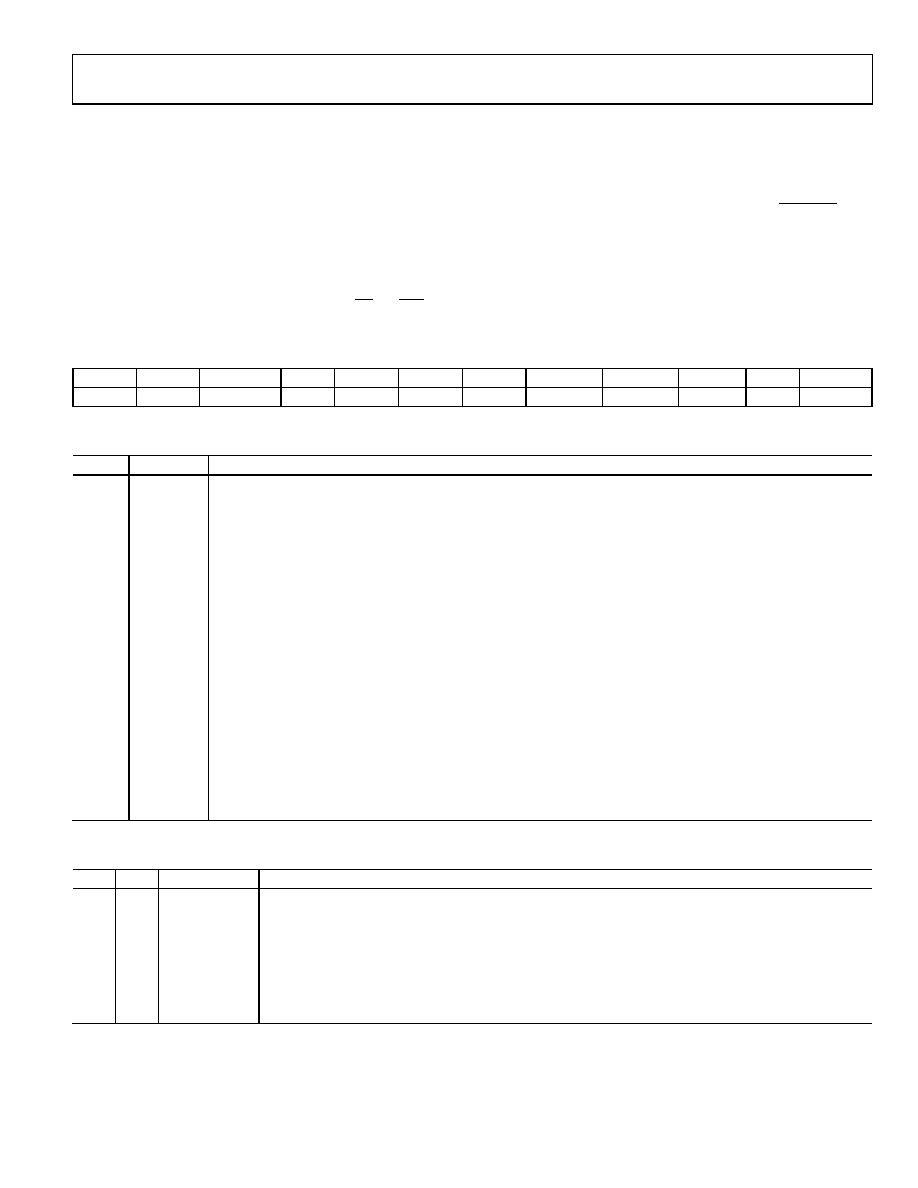
Table 6. Control Register Bits
MSB
LSB
DB11
DB10
DB9
DB8
DB7
DB6
DB5
DB4
DB3
DB2
DB1
DB0
PM1
PM0
CODING
REF
ADD2
ADD1
ADD0
MODE1
MODE0
SHDW
SEQ
RANGE
Table 7. Control Register Bit Function Description
Bit No.
Mnemonic
Description
11, 10
PM1, PM0
Power Management Bits. These two bits are used to select the power mode of operation. The user can choose
between either normal mode or various power-down modes of operation as shown in Table 8.
9
CODING
This bit selects the output coding of the conversion result. If this bit is set to 0, the output coding is straight
(natural) binary. If this bit is set to 1, the output coding is twos complement.
8
REF
This bit selects whether the internal or external reference is used to perform the conversion. If this bit is Logic 0, an
external reference should be applied to the VREF pin. If this bit is Logic 1, the internal reference is selected. See the
Reference section.
7 to 5
ADD2 to
ADD0
These three address bits are used to either select which analog input channel is converted in the next conversion if
the sequencer is not used, or to select the final channel in a consecutive sequence when the sequencer is used as
4, 3
MODE1,
MODE0
The two mode pins select the type of analog input on the eight VIN pins. The AD7938-6 can have either eight single-
ended inputs, four fully differential inputs, four pseudo differential inputs, or seven pseudo differential inputs. See
2
SHDW
The SHDW bit in the control register is used in conjunction with the SEQ bit to control the sequencer function and
access the SHDW register. See Table 10.
1
SEQ
The SEQ bit in the control register is used in conjunction with the SHDW bit to control the sequencer function and
access the SHDW register. See Table 10.
0
RANGE
This bit selects the analog input range of the AD7938-6. If it is set to 0, then the analog input range extends from
0 V to VREF. If it is set to 1, the analog input range extends from 0 V to 2 × VREF. When this range is selected, VDD must
be 4.75 V to 5.25 V if a 2.5 V reference is used; otherwise, care must be taken to ensure that the analog input remains
within the supply rails. See the Analog Inputs section for more information.
Table 8. Power Mode Selection using the Power Management Bits in the Control Register
PM1
PM0
Mode
Description
0
Normal Mode
When operating in normal mode, all circuitry is fully powered up at all times.
0
1
Autoshutdown
When operating in autoshutdown mode, the AD7938-6 enters full shutdown mode at the end of each
conversion. In this mode, all circuitry is powered down.
1
0
Autostandby
When the AD7938-6 enters this mode, all circuitry is powered down except for the reference and reference
buffer. This mode is similar to autoshutdown mode, but it allows the part to power up in 7 μs (or 600 ns if
an external reference is used). See the Power Modes of Operation section for more information.
1
Full Shutdown
When the AD7938-6 enters this mode, all circuitry is powered down. The information in the control register
is retained.
相关PDF资料 |
PDF描述 |
|---|---|
| AD7938BCPZ | IC ADC 12BIT 8CH 1.5MSPS 32LFCSP |
| AD7940BRM | IC ADC 14BIT UNIPOLAR 8-MSOP |
| AD7942BRMZ-RL7 | IC ADC 14BIT 250KSPS 10-MSOP |
| AD7944BCPZ | IC ADC 14BIT 2.5MSPS 20LFCSP |
| AD7946BCPZRL7 | IC ADC 14BIT 500KSPS 10-LFCSP |
相关代理商/技术参数 |
参数描述 |
|---|---|
| AD7938BCPZ-6REEL7 | 功能描述:IC ADC 12BIT 8CH 625KSPS 32LFCSP RoHS:是 类别:集成电路 (IC) >> 数据采集 - 模数转换器 系列:- 标准包装:1,000 系列:- 位数:16 采样率(每秒):45k 数据接口:串行 转换器数目:2 功率耗散(最大):315mW 电压电源:模拟和数字 工作温度:0°C ~ 70°C 安装类型:表面贴装 封装/外壳:28-SOIC(0.295",7.50mm 宽) 供应商设备封装:28-SOIC W 包装:带卷 (TR) 输入数目和类型:2 个单端,单极 |
| AD7938BCPZ-REEL7 | 功能描述:IC ADC 12BIT 8CH 1.5MSPS 32LFCSP RoHS:是 类别:集成电路 (IC) >> 数据采集 - 模数转换器 系列:- 标准包装:1,000 系列:- 位数:12 采样率(每秒):300k 数据接口:并联 转换器数目:1 功率耗散(最大):75mW 电压电源:单电源 工作温度:0°C ~ 70°C 安装类型:表面贴装 封装/外壳:24-SOIC(0.295",7.50mm 宽) 供应商设备封装:24-SOIC 包装:带卷 (TR) 输入数目和类型:1 个单端,单极;1 个单端,双极 |
| AD7938BSU | 制造商:Analog Devices 功能描述: |
| AD7938BSU-6 | 制造商:Analog Devices 功能描述:ADC Single SAR 625ksps 12-bit Parallel 32-Pin TQFP |
| AD7938BSU-6REEL | 制造商:AD 制造商全称:Analog Devices 功能描述:8-Channel, 625 kSPS, 12-Bit Parallel ADCs with a Sequencer |
发布紧急采购,3分钟左右您将得到回复。