- 您现在的位置:买卖IC网 > PDF目录10258 > AD7938BSUZ-6 (Analog Devices Inc)IC ADC 12BIT 8CHAN 32TQFP PDF资料下载
参数资料
| 型号: | AD7938BSUZ-6 |
| 厂商: | Analog Devices Inc |
| 文件页数: | 30/32页 |
| 文件大小: | 0K |
| 描述: | IC ADC 12BIT 8CHAN 32TQFP |
| 标准包装: | 1 |
| 位数: | 12 |
| 采样率(每秒): | 625k |
| 数据接口: | 并联 |
| 转换器数目: | 1 |
| 功率耗散(最大): | 7.5mW |
| 电压电源: | 单电源 |
| 工作温度: | -40°C ~ 85°C |
| 安装类型: | 表面贴装 |
| 封装/外壳: | 32-TQFP |
| 供应商设备封装: | 32-TQFP(7x7) |
| 包装: | 托盘 |
| 输入数目和类型: | 8 个单端,单极;4 个差分,单极;4 个伪差分,单极;7 伪差分,单极 |
| 配用: | EVAL-AD7938CBZ-ND - EVAL BOARD FOR AD7938 |
第1页第2页第3页第4页第5页第6页第7页第8页第9页第10页第11页第12页第13页第14页第15页第16页第17页第18页第19页第20页第21页第22页第23页第24页第25页第26页第27页第28页第29页当前第30页第31页第32页
Data Sheet
AD7938-6
Rev. C | Page 7 of 32
04
751
-00
6
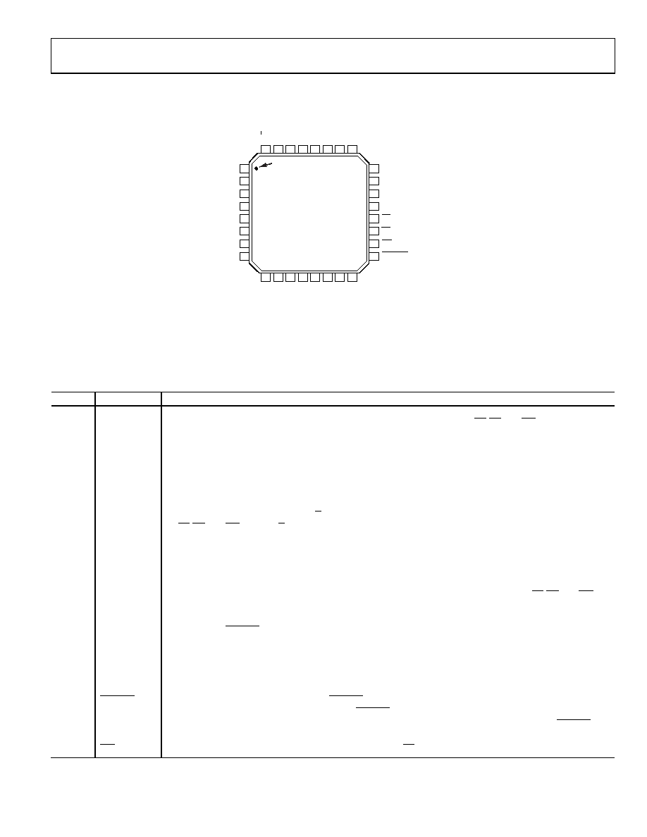
PIN CONFIGURATION AND FUNCTION DESCRIPTIONS
DB0 1
V
DR
IV
E
9
DG
ND
10
DB
8/
HBE
N
11
DB9
12
DB
10
13
DB
11
14
BUS
Y
15
CL
KI
N
16
W/B
32
V
DD
31
V
IN
7
30
V
IN
6
29
V
IN
5
28
V
IN
4
27
V
IN
3
26
V
IN
2
25
DB1 2
DB2 3
DB3 4
DB4 5
DB5 6
DB6 7
DB7 8
VIN1
24
VIN0
23
VREFIN/VREFOUT
22
AGND
21
20
19
WR
18
CONVST
17
AD7938-6
TOP VIEW
(Not to Scale)
RD
CS
PIN 1
IDENTIFIER
NOTES
1. THE EXPOSED PAD IS LOCATED ON THE UNDERSIDE OF
THE PACKAGE. CONNECT THE EPAD TO THE GROUND PLANE
OF THE PCB USING MULTIPLE VIAS.
Figure 2. Pin Configuration
Table 5. Pin Function Description
Pin No.
Mnemonic
Description
1 to 8
DB0 to DB7
Data Bit 0 to Data Bit 7. Three-state parallel digital I/O pins that provide the conversion result and allow the
control and shadow registers to be programmed. These pins are controlled by CS, RD, and WR. The logic
high/low voltage levels for these pins are determined by the VDRIVE input.
9
VDRIVE
Logic Power Supply Input. The voltage supplied at this pin determines at what voltage the parallel interface of
the AD7938-6 operates. This pin should be decoupled to DGND. The voltage at this pin may be different to that
at VDD but should never exceed VDD by more than 0.3 V.
10
DGND
Digital Ground. This is the ground reference point for all digital circuitry on the AD7938-6. This pin should
connect to the DGND plane of a system. The DGND and AGND voltages should ideally be at the same potential
and must not be more than 0.3 V apart, even on a transient basis.
11
DB8/HBEN
Data Bit 8/High Byte Enable. When W/B is high, this pin acts as Data Bit 8, a three-state I/O pin that is controlled
by CS, RD, and WR. When W/B is low, this pin acts as the high byte enable pin. When HBEN is low, the low byte of
data being written to or read from the AD7938-6 is on DB0 to DB7. When HBEN is high, the top four bits of the
data being written to or read from the AD7938-6 are on DB0 to DB3. When reading from the device, DB4 to DB6
of the high byte contains the ID of the channel to which the conversion result corresponds (see the channel
address bits in
). When writing to the device, DB4 to DB7 of the high byte must be all 0s.
12 to 14
DB9 to DB11
Data Bit 9 to Data Bit 11. Three-state parallel digital I/O pins that provide the conversion result and allow the
control and shadow registers to be programmed in word mode. These pins are controlled by CS, RD, and WR.
The logic high/low voltage levels for these pins are determined by the VDRIVE input.
15
BUSY
Busy Output. Logic output indicating the status of the conversion. The BUSY output goes high following the
falling edge of CONVST and stays high for the duration of the conversion. Once the conversion is complete and
the result is available in the output register, the BUSY output goes low. The track-and-hold returns to track mode
just prior to the falling edge of BUSY on the 13th rising edge of CLKIN (see
).
16
CLKIN
Master Clock Input. The clock source for the conversion process is applied to this pin. Conversion time for the
AD7938-6 takes 13 clock cycles + t2. The frequency of the master clock input therefore determines the
conversion time and achievable throughput rate. The CLKIN signal may be a continuous or burst clock.
17
CONVST
Conversion Start Input. A falling edge on CONVST is used to initiate a conversion. The track-and-hold goes from
track mode to hold mode on the falling edge of CONVST and the conversion process is initiated at this point.
Following power-down, when operating in autoshutdown or autostandby modes, a rising edge on CONVST is
used to power up the device.
18
WR
Write Input. Active low logic input used in conjunction with CS to write data to the internal registers.
相关PDF资料 |
PDF描述 |
|---|---|
| VI-BNW-MW-S | CONVERTER MOD DC/DC 5.5V 100W |
| VI-240-IU-S | CONVERTER MOD DC/DC 5V 200W |
| MS3102A32-9S | CONN RCPT 14POS BOX MNT W/SCKT |
| MS27474T20A35P | CONN RCPT 79POS JAM NUT W/PINS |
| MS27473E8F98SA | CONN PLUG 3POS STRAIGHT W/SCKT |
相关代理商/技术参数 |
参数描述 |
|---|---|
| AD7938BSUZ-6REEL7 | 功能描述:IC ADC 12BIT 8CHAN 32TQFP RoHS:是 类别:集成电路 (IC) >> 数据采集 - 模数转换器 系列:- 其它有关文件:TSA1204 View All Specifications 标准包装:1 系列:- 位数:12 采样率(每秒):20M 数据接口:并联 转换器数目:2 功率耗散(最大):155mW 电压电源:模拟和数字 工作温度:-40°C ~ 85°C 安装类型:表面贴装 封装/外壳:48-TQFP 供应商设备封装:48-TQFP(7x7) 包装:Digi-Reel® 输入数目和类型:4 个单端,单极;2 个差分,单极 产品目录页面:1156 (CN2011-ZH PDF) 其它名称:497-5435-6 |
| AD7938BSUZ-REEL7 | 功能描述:IC ADC 12BIT 8CHAN 32TQFP RoHS:是 类别:集成电路 (IC) >> 数据采集 - 模数转换器 系列:- 标准包装:1,000 系列:- 位数:12 采样率(每秒):300k 数据接口:并联 转换器数目:1 功率耗散(最大):75mW 电压电源:单电源 工作温度:0°C ~ 70°C 安装类型:表面贴装 封装/外壳:24-SOIC(0.295",7.50mm 宽) 供应商设备封装:24-SOIC 包装:带卷 (TR) 输入数目和类型:1 个单端,单极;1 个单端,双极 |
| AD7939 | 制造商:AD 制造商全称:Analog Devices 功能描述:8-Channel, 1.5 MSPS, 12-Bit and 10-Bit Parallel ADCs with a Sequencer |
| AD7939BCP | 制造商:Analog Devices 功能描述:ADC Single SAR 1.5Msps 10-bit Parallel 32-Pin LFCSP EP |
| AD7939BCP-REEL | 制造商:Analog Devices 功能描述:ADC SGL SAR 1.5MSPS 10-BIT PARALLEL 32LFCSP EP - Tape and Reel |
发布紧急采购,3分钟左右您将得到回复。