- 您现在的位置:买卖IC网 > PDF目录294844 > AD7942 (Analog Devices, Inc.) 14-Bit, 250 kSPS PulSAR ADC in MSOP/QFN PDF资料下载
参数资料
| 型号: | AD7942 |
| 厂商: | Analog Devices, Inc. |
| 元件分类: | ADC |
| 英文描述: | 14-Bit, 250 kSPS PulSAR ADC in MSOP/QFN |
| 中文描述: | 14位,250 kSPS的PulSAR系列ADC的,采用MSOP / QFN封装 |
| 文件页数: | 7/28页 |
| 文件大小: | 633K |
| 代理商: | AD7942 |
第1页第2页第3页第4页第5页第6页当前第7页第8页第9页第10页第11页第12页第13页第14页第15页第16页第17页第18页第19页第20页第21页第22页第23页第24页第25页第26页第27页第28页
Preliminary Technical Data
AD7942
Rev Pr B | Page 15 of 28
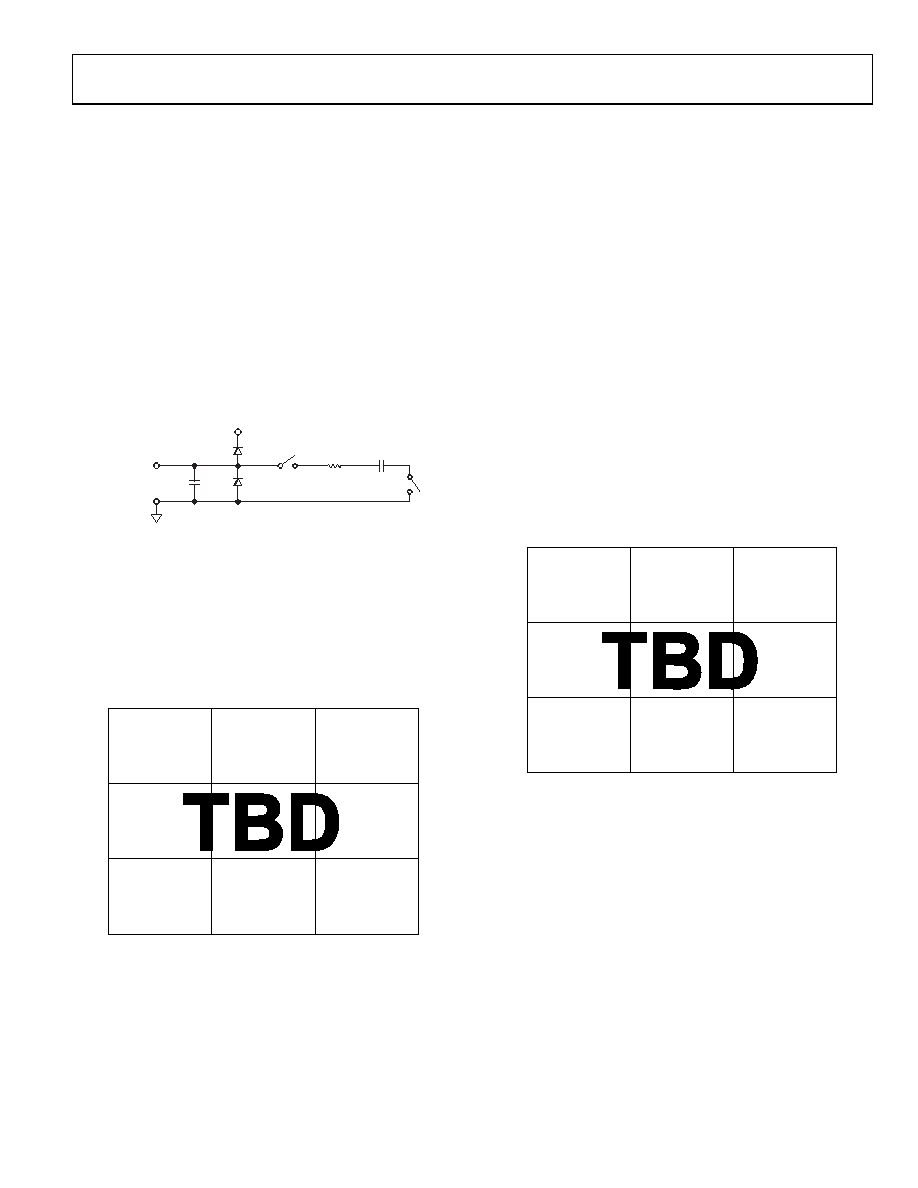
Analog Input
Figure 23 shows an equivalent circuit of the input structure of
the AD7942.
The two diodes, D1 and D2, provide ESD protection for the
analog inputs IN+ and IN. Care must be taken to ensure that
the analog input signal never exceeds the supply rails by more
than 0.3 V because this will cause these diodes to become
forward-biased and start conducting current. However, these
diodes can handle a forward-biased current of 130 mA
maximum. For instance, these conditions could eventually
occur when the input buffer’s (U1) supplies are different from
VDD. In such a case, an input buffer with a short-circuit current
limitation can be used to protect the part.
CIN
RIN
D1
D2
CPIN
IN+
OR IN–
GND
VDD
Figure 23. Equivalent Analog Input Circuit
This analog input structure allows the sampling of the
differential signal between IN+ and IN. By using this
differential input, small signals common to both inputs are
rejected, as shown in Figure 24, which represents the typical
CMRR over frequency. For instance, by using IN to sense a
remote signal ground, ground potential differences between the
sensor and the local ADC ground are eliminated.
Figure 24. Analog Input CMRR vs. Frequency
During the acquisition phase, the impedance of the analog
input IN+ can be modeled as a parallel combination of
capacitor CPIN and the network formed by the series connection
of RIN and CIN. CPIN is primarily the pin capacitance. RIN is
typically 3 k and is a lumped component made up of some
serial resistors and the on resistance of the switches. CIN is
typically 30 pF and is mainly the ADC sampling capacitor.
During the conversion phase, where the switches are opened,
the input impedance is limited to CPIN. RIN and CIN make a 1-
pole, low-pass filter that reduces undesirable aliasing effect and
limits the noise.
When the source impedance of the driving circuit is low, the
AD7942 can be driven directly. Large source impedances
significantly affect the ac performance, especially total
harmonic distortion (THD). The dc performances are less
sensitive to the input impedance. The maximum source
impedance depends on the amount of THD that can be
tolerated. The THD degrades as a function of the source
impedance and the maximum input frequency, as shown in
Figure 25. THD vs. Analog Input Frequency and Source Resistance
相关PDF资料 |
PDF描述 |
|---|---|
| AD7943BN | +3.3 V/+5 V Multiplying 12-Bit DACs |
| AD7943BR | +3.3 V/+5 V Multiplying 12-Bit DACs |
| AD7943BRS | +3.3 V/+5 V Multiplying 12-Bit DACs |
| AD7945BN | +3.3 V/+5 V Multiplying 12-Bit DACs |
| AD7945BR | +3.3 V/+5 V Multiplying 12-Bit DACs |
相关代理商/技术参数 |
参数描述 |
|---|---|
| AD79421 | 制造商:AD 制造商全称:Analog Devices 功能描述:18-Bit, 2 MSPS PulSAR 15 mW ADC in LFCSP (QFN) |
| AD7942BCPRL7 | 制造商:AD 制造商全称:Analog Devices 功能描述:14-Bit, 250 kSPS PulSAR ADC in MSOP/QFN |
| AD7942BCPWP | 制造商:AD 制造商全称:Analog Devices 功能描述:14-Bit, 250 kSPS PulSAR ADC in MSOP/QFN |
| AD7942BCPZRL | 功能描述:IC ADC 14BIT SAR 250KSPS 10LFCSP RoHS:是 类别:集成电路 (IC) >> 数据采集 - 模数转换器 系列:PulSAR® 标准包装:1,000 系列:- 位数:16 采样率(每秒):45k 数据接口:串行 转换器数目:2 功率耗散(最大):315mW 电压电源:模拟和数字 工作温度:0°C ~ 70°C 安装类型:表面贴装 封装/外壳:28-SOIC(0.295",7.50mm 宽) 供应商设备封装:28-SOIC W 包装:带卷 (TR) 输入数目和类型:2 个单端,单极 |
| AD7942BCPZRL1 | 制造商:AD 制造商全称:Analog Devices 功能描述:14-Bit, 250 kSPS PulSAR, Pseudo Differential ADC in MSOP/QFN |
发布紧急采购,3分钟左右您将得到回复。