- 您现在的位置:买卖IC网 > PDF目录10566 > AD7942BCPZRL7 (Analog Devices Inc)IC ADC 14BIT 250KSPS 10-LFCSP PDF资料下载
参数资料
| 型号: | AD7942BCPZRL7 |
| 厂商: | Analog Devices Inc |
| 文件页数: | 11/24页 |
| 文件大小: | 0K |
| 描述: | IC ADC 14BIT 250KSPS 10-LFCSP |
| 标准包装: | 1 |
| 系列: | PulSAR® |
| 位数: | 14 |
| 采样率(每秒): | 250k |
| 数据接口: | DSP,MICROWIRE?,QSPI?,串行,SPI? |
| 转换器数目: | 1 |
| 功率耗散(最大): | 1.25mW |
| 电压电源: | 单电源 |
| 工作温度: | -40°C ~ 85°C |
| 安装类型: | 表面贴装 |
| 封装/外壳: | 10-WFDFN 裸露焊盘,CSP |
| 供应商设备封装: | 10-LFCSP-WD(3x3) |
| 包装: | 标准包装 |
| 输入数目和类型: | 1 个伪差分,单极 |
| 配用: | EVAL-AD7942CB-ND - BOARD EVALUATION FOR AD7942 |
| 其它名称: | AD7942BCPZRL7DKR |
AD7942
Rev. B | Page 19 of
24
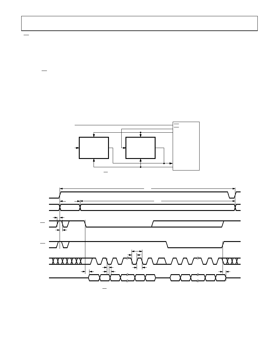
CS Mode 4-Wire Without Busy Indicator
This mode is most often used when multiple AD7942s are
connected to an SPI-compatible digital host. A connection
diagram using two AD7942s is shown in Figure 34 and the
corresponding timing diagram is given in Figure 35.
With SDI high, a rising edge on CNV initiates a conversion,
selects the CS mode, and forces SDO to high impedance. In this
mode, CNV must be held high during the conversion phase and
the subsequent data readback (if SDI and CNV are low, SDO is
driven low). Prior to the minimum conversion time, SDI can be
used to select other SPI devices, such as analog multiplexers.
However, SDI must be returned high before the minimum
conversion time elapses and held high until the maximum
conversion time is completed to avoid generating the busy
signal indicator. When the conversion is complete, the AD7942
enters the acquisition phase and powers down. Each ADC result
can be read by bringing its SDI input low, which consequently
outputs the MSB onto SDO. The remaining data bits are then
clocked by subsequent SCK driving edges. The data is valid on
both SCK edges. Although the nondriving edge can be used to
capture the data, a digital host also using the SCK falling edge
allows a faster reading rate, provided it has an acceptable hold
time. After the 14th SCK falling edge or when SDI goes high,
whichever is earlier, SDO returns to high impedance and
another AD7942 can be read.
If multiple AD7942s are selected at the same time, the SDO
output pin handles this contention without damage or induced
latch-up. Meanwhile, it is recommended to keep this contention
as short as possible to limit extra power dissipation.
CNV
SCK
SDO
SDI
DATA IN
CLK
CS1
CONVERT
CS2
DIGITAL HOST
AD7942
CNV
SCK
SDO
SDI
AD7942
04
65
7-
03
4
Figure 34. CS Mode 4-Wire Without Busy Indicator Connection Diagram
SDO
D13
D12
D11
D1
D0
tDIS
SCK
12
3
26
27
28
tHSDO
tDSDO
tEN
CONVERSION
ACQUISITION
tCONV
tCYC
tACQ
ACQUISITION
SDI (CS1)
CNV
tSSDICNV
tHSDICNV
D1
12
13
tSCK
tSCKL
tSCKH
D0
D13
D12
15
16
14
SDI (CS2)
04
65
7-
0
35
Figure 35. CS Mode 4-Wire Without Busy Indicator, Serial Interface Timing
相关PDF资料 |
PDF描述 |
|---|---|
| VE-251-IW-F4 | CONVERTER MOD DC/DC 12V 100W |
| VI-25X-MX | CONVERTER MOD DC/DC 5.2V 75W |
| VE-251-IW-F2 | CONVERTER MOD DC/DC 12V 100W |
| VE-251-IW-F1 | CONVERTER MOD DC/DC 12V 100W |
| MAX11617EEE+ | IC ADC SERIAL 12BIT 12CH 16-QSOP |
相关代理商/技术参数 |
参数描述 |
|---|---|
| AD7942BCPZRL71 | 制造商:AD 制造商全称:Analog Devices 功能描述:14-Bit, 250 kSPS PulSAR, Pseudo Differential ADC in MSOP/QFN |
| AD7942BRM | 制造商:Analog Devices 功能描述:ADC Single SAR 250ksps 14-bit Serial 10-Pin MSOP Tube 制造商:Analog Devices 功能描述:IC 14-BIT ADC |
| AD7942BRMRL7 | 制造商:AD 制造商全称:Analog Devices 功能描述:14-Bit, 250 kSPS PulSAR ADC in MSOP/QFN |
| AD7942BRM-RL7 | 制造商:Analog Devices 功能描述:ADC Single SAR 250ksps 14-bit Serial 10-Pin MSOP T/R |
| AD7942BRMZ | 功能描述:IC ADC 14BIT 250KSPS 10-MSOP RoHS:是 类别:集成电路 (IC) >> 数据采集 - 模数转换器 系列:PulSAR® 标准包装:1 系列:microPOWER™ 位数:8 采样率(每秒):1M 数据接口:串行,SPI? 转换器数目:1 功率耗散(最大):- 电压电源:模拟和数字 工作温度:-40°C ~ 125°C 安装类型:表面贴装 封装/外壳:24-VFQFN 裸露焊盘 供应商设备封装:24-VQFN 裸露焊盘(4x4) 包装:Digi-Reel® 输入数目和类型:8 个单端,单极 产品目录页面:892 (CN2011-ZH PDF) 其它名称:296-25851-6 |
发布紧急采购,3分钟左右您将得到回复。