参数资料
| 型号: | AD7942BRMZ-RL7 |
| 厂商: | Analog Devices Inc |
| 文件页数: | 6/24页 |
| 文件大小: | 0K |
| 描述: | IC ADC 14BIT 250KSPS 10-MSOP |
| 标准包装: | 1,000 |
| 系列: | PulSAR® |
| 位数: | 14 |
| 采样率(每秒): | 250k |
| 数据接口: | DSP,MICROWIRE?,QSPI?,串行,SPI? |
| 转换器数目: | 1 |
| 功率耗散(最大): | 1.25mW |
| 电压电源: | 单电源 |
| 工作温度: | -40°C ~ 85°C |
| 安装类型: | 表面贴装 |
| 封装/外壳: | 10-TFSOP,10-MSOP(0.118",3.00mm 宽) |
| 供应商设备封装: | 10-MSOP |
| 包装: | 带卷 (TR) |
| 输入数目和类型: | 1 个伪差分,单极 |
| 配用: | EVAL-AD7942CB-ND - BOARD EVALUATION FOR AD7942 |
AD7942
Rev. B | Page 14 of
24
AD7942
REF
GND
VDD
IN–
IN+
VIO
SDI
SCK
SDO
CNV
3- OR 4-WIRE INTERFACE (NOTE 5)
100nF
5V
10F
(NOTE 2)
1.8V TO VDD
REF
0V TO VREF
33
2.7nF
(NOTE 3)
(NOTE 4)
(NOTE 1)
NOTE 1: SEE THE VOLTAGE REFERENCE INPUT SECTION FOR REFERENCE SELECTION.
NOTE 2: CREF IS USUALLY A 10F CERAMIC CAPACITOR (X5R).
NOTE 3: SEE DRIVER AMPLIFIER CHOICE SECTION.
NOTE 4: OPTIONAL FILTER. SEE ANALOG INPUT SECTION.
NOTE 5: SEE DIGITAL INTERFACE FOR MOST CONVENIENT INTERFACE MODE.
04
65
7-
02
2
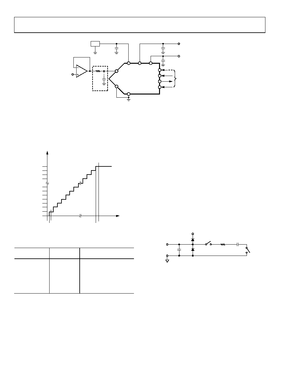
Figure 22. Typical Application Diagram
Transfer Functions
The ideal transfer characteristic for the AD7942 is shown in
000...000
000...001
000...010
111...101
111...110
111...111
ADC
CO
DE
(
S
T
RAI
G
HT
BI
N
A
R
Y)
ANALOG INPUT
+FS – 1.5 LSB
+
FS – 1 LSB
–FS + 1 LSB
–FS
–FS + 0.5 LSB
04
65
7-
02
3
Figure 23. ADC Ideal Transfer Function
Table 7. Output Codes and Ideal Input Voltages
Description
Analog Input
VREF = 5 V
Digital Output Code
Hexadecimal
FSR – 1 LSB
4.999695 V
Midscale + 1 LSB
2.500305 V
0x2001
Midscale
2.5 V
0x2000
Midscale – 1 LSB
2.499695 V
0x1FFF
–FSR + 1 LSB
305.2 μV
0x0001
–FSR
0 V
1 This is also the code for an overranged analog input (VIN+ – VIN > VREF – VGND).
2 This is also the code for an underranged analog input (VIN+ – VIN < VGND).
TYPICAL CONNECTION DIAGRAM
Figure 22 shows an example of the recommended connection
diagram for the AD7942 when multiple supplies are available.
Analog Input
Figure 24 shows an equivalent circuit of the input structure of
the AD7942.
The two diodes, D1 and D2, provide ESD protection for the
analog inputs, IN+ and IN. Care must be taken to ensure that
the analog input signal never exceeds the supply rails by more
than 0.3 V because this causes these diodes to become forward-
biased and to start conducting current. However, these diodes
can handle a forward-biased current of 130 mA maximum. For
instance, these conditions could eventually occur when the
input buffer (U1) supplies are different from VDD. In such a
case, an input buffer with a short-circuit current limitation can
be used to protect the part.
CIN
RIN
D1
D2
CPIN
IN+
OR IN–
GND
VDD
04
65
7-
02
4
Figure 24. Equivalent Analog Input Circuit
This analog input structure allows the sampling of the diffe-
rential signal between IN+ and IN. By using this differential
input, small signals common to both inputs are rejected, as
shown in Figure 25, which represents the typical CMRR over
frequency. For instance, by using IN to sense a remote signal
ground, ground potential differences between the sensor and
the local ADC ground are eliminated.
相关PDF资料 |
PDF描述 |
|---|---|
| AD7944BCPZ | IC ADC 14BIT 2.5MSPS 20LFCSP |
| AD7946BCPZRL7 | IC ADC 14BIT 500KSPS 10-LFCSP |
| AD7948BN | IC DAC 12BIT MULT PARALL 20-DIP |
| AD7949BCPZRL7 | IC ADC 14BIT 250KSPS 8CH 20LFCSP |
| AD7951BSTZRL | IC ADC 14BIT 1MSPS 48-LQFP |
相关代理商/技术参数 |
参数描述 |
|---|---|
| AD7942BRMZ-RL71 | 制造商:AD 制造商全称:Analog Devices 功能描述:14-Bit, 250 kSPS PulSAR, Pseudo Differential ADC in MSOP/QFN |
| AD7943 | 制造商:AD 制造商全称:Analog Devices 功能描述:+3.3 V/+5 V Multiplying 12-Bit DACs |
| AD7943AN-B | 制造商:Rochester Electronics LLC 功能描述:SERIAL 12-BIT IOUT DAC-IC - Bulk |
| AD7943ANZ-B | 功能描述:IC DAC 12BIT MULT SRL 16DIP RoHS:是 类别:集成电路 (IC) >> 数据采集 - 数模转换器 系列:- 标准包装:47 系列:- 设置时间:2µs 位数:14 数据接口:并联 转换器数目:1 电压电源:单电源 功率耗散(最大):55µW 工作温度:-40°C ~ 85°C 安装类型:表面贴装 封装/外壳:28-SSOP(0.209",5.30mm 宽) 供应商设备封装:28-SSOP 包装:管件 输出数目和类型:1 电流,单极;1 电流,双极 采样率(每秒):* |
| AD7943ARSB | 制造商:Analog Devices 功能描述: |
发布紧急采购,3分钟左右您将得到回复。