- 您现在的位置:买卖IC网 > PDF目录10212 > AD7952BCPZRL (Analog Devices Inc)IC ADC 14BIT DIFF 1MSPS 48LFCSP PDF资料下载
参数资料
| 型号: | AD7952BCPZRL |
| 厂商: | Analog Devices Inc |
| 文件页数: | 16/32页 |
| 文件大小: | 0K |
| 描述: | IC ADC 14BIT DIFF 1MSPS 48LFCSP |
| 标准包装: | 2,500 |
| 系列: | PulSAR® |
| 位数: | 14 |
| 采样率(每秒): | 1M |
| 数据接口: | 串行,并联 |
| 转换器数目: | 1 |
| 功率耗散(最大): | 260mW |
| 电压电源: | 模拟和数字,双 ± |
| 工作温度: | -40°C ~ 85°C |
| 安装类型: | 表面贴装 |
| 封装/外壳: | 48-VFQFN 裸露焊盘,CSP |
| 供应商设备封装: | 48-LFCSP-VQ(7x7) |
| 包装: | 带卷 (TR) |
| 输入数目和类型: | 1 个差分,双极 |
第1页第2页第3页第4页第5页第6页第7页第8页第9页第10页第11页第12页第13页第14页第15页当前第16页第17页第18页第19页第20页第21页第22页第23页第24页第25页第26页第27页第28页第29页第30页第31页第32页
Data Sheet
AD7952
Rev. A | Page 23 of 32
OVDD should be set to the same level as the system interface.
Sufficient decoupling is required, consisting of at least a 10 μF
capacitor and a 100 nF capacitor with the 100 nF capacitors
placed as close as possible to the AD7952.
Power Sequencing
The AD7952 requires sequencing of the AVDD and DVDD
supplies. AVDD should come up prior to or simultaneously
with DVDD. This can be achieved using the configuration in
Figure 27 or sequencing the supplies in that manner. The
other supplies can be sequenced as desired as long as absolute
maximum ratings are observed. The AD7952 is very insensitive
to power supply variations on AVDD over a wide frequency
range, as shown in Figure 32.
80
75
1
10000
FREQUENCY (kHz)
PS
R
(d
B)
10
100
1000
70
65
60
55
50
45
40
35
30
EXT REF
INT REF
0
65
89-
0
31
Figure 32. AVDD PSRR vs. Frequency
Power Dissipation vs. Throughput
In impulse mode, the AD7952 automatically reduces its power
consumption at the end of each conversion phase. During the
acquisition phase, the operating currents are very low, which allows
a significant power savings when the conversion rate is reduced
(see Figure 33). This feature makes the AD7952 ideal for very
low power, battery-operated applications.
It should be noted that the digital interface remains active even
during the acquisition phase. To reduce the operating digital supply
currents even further, drive the digital inputs close to the power
rails (that is, OVDD and OGND).
1000
1
10
1000000
P
O
W
E
R
DI
S
IP
AT
IO
N
(m
W
)
100
10
100
1000
10000
100000
PDREF = PDBUF = HIGH
WARP MODE POWER
IMPULSE MODE POWER
06
589
-03
2
Figure 33. Power Dissipation vs. Sample Rate
Power Down
Setting PD = high powers down the AD7952, thus reducing
supply currents to their minimums, as shown in Figure 23. When
the ADC is in power-down, the current conversion (if any) is
completed and the digital bus remains active. To further reduce
the digital supply currents, drive the inputs to OVDD or OGND.
Power-down can also be programmed with the configuration
register. See the Software Configuration section for details. Note
that when using the configuration register, the PD input is a
don’t care and should be tied to either high or low.
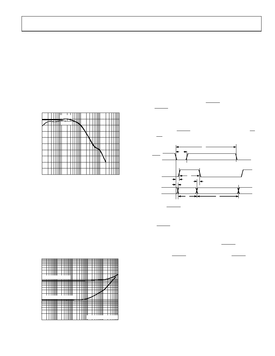
CONVERSION CONTROL
The AD7952 is controlled by the CNVST input. A falling edge
on CNVST is all that is necessary to initiate a conversion. A
detailed timing diagram of the conversion process is shown in
Figure 34. Once initiated, it cannot be restarted or aborted,
even by the power-down input, PD, until the conversion is
completed. The CNVST signal operates independently of the CS
and RD signals.
BUSY
MODE
CONVERT
ACQUIRE
CONVERT
CNVST
t1
t2
t4
t3
t5
t6
t7
t8
0
65
89
-03
3
Figure 34. Basic Conversion Timing
Although CNVST is a digital signal, it should be designed with
special care with fast, clean edges, and levels with minimum
overshoot, undershoot, or ringing.
The CNVST trace should be shielded with ground, and a low value
(such as 50 Ω) serial resistor termination should be added close
to the output of the component that drives this line.
For applications where SNR is critical, the CNVST signal should
have very low jitter. This can be achieved by using a dedicated
oscillator for CNVST generation, or by clocking CNVST with a
high frequency, low jitter clock, as shown in Figure 27.
相关PDF资料 |
PDF描述 |
|---|---|
| SP3071EEN-L/TR | IC TXRX RS485/RS422 ESD 8NSOIC |
| AD7492BR-REEL7 | IC ADC 12BIT W/REF W/CLK 24-SOIC |
| ADM101EARMZ-REEL | IC TXRX RS-232 SINGLE 5V 10MSOP |
| VE-B1F-MY | CONVERTER MOD DC/DC 72V 50W |
| VE-B1D-MY | CONVERTER MOD DC/DC 85V 50W |
相关代理商/技术参数 |
参数描述 |
|---|---|
| AD7952BSTZ | 功能描述:IC ADC 14BIT DIFF 1MSPS 48-LQFP RoHS:是 类别:集成电路 (IC) >> 数据采集 - 模数转换器 系列:PulSAR® 其它有关文件:TSA1204 View All Specifications 标准包装:1 系列:- 位数:12 采样率(每秒):20M 数据接口:并联 转换器数目:2 功率耗散(最大):155mW 电压电源:模拟和数字 工作温度:-40°C ~ 85°C 安装类型:表面贴装 封装/外壳:48-TQFP 供应商设备封装:48-TQFP(7x7) 包装:Digi-Reel® 输入数目和类型:4 个单端,单极;2 个差分,单极 产品目录页面:1156 (CN2011-ZH PDF) 其它名称:497-5435-6 |
| AD7952BSTZRL | 功能描述:IC ADC 14BIT DIFF 1MSPS 48-LQFP RoHS:是 类别:集成电路 (IC) >> 数据采集 - 模数转换器 系列:PulSAR® 标准包装:1,000 系列:- 位数:12 采样率(每秒):300k 数据接口:并联 转换器数目:1 功率耗散(最大):75mW 电压电源:单电源 工作温度:0°C ~ 70°C 安装类型:表面贴装 封装/外壳:24-SOIC(0.295",7.50mm 宽) 供应商设备封装:24-SOIC 包装:带卷 (TR) 输入数目和类型:1 个单端,单极;1 个单端,双极 |
| AD795AH | 制造商:未知厂家 制造商全称:未知厂家 功能描述:Voltage-Feedback Operational Amplifier |
| AD795BH | 制造商:未知厂家 制造商全称:未知厂家 功能描述:Voltage-Feedback Operational Amplifier |
| AD795JN | 制造商:Analog Devices 功能描述:Operational Amplifier, Single AMP, Bipolar/JFET, 8 Pin, Plastic, DIP |
发布紧急采购,3分钟左右您将得到回复。