- 您现在的位置:买卖IC网 > PDF目录10212 > AD7952BCPZRL (Analog Devices Inc)IC ADC 14BIT DIFF 1MSPS 48LFCSP PDF资料下载
参数资料
| 型号: | AD7952BCPZRL |
| 厂商: | Analog Devices Inc |
| 文件页数: | 18/32页 |
| 文件大小: | 0K |
| 描述: | IC ADC 14BIT DIFF 1MSPS 48LFCSP |
| 标准包装: | 2,500 |
| 系列: | PulSAR® |
| 位数: | 14 |
| 采样率(每秒): | 1M |
| 数据接口: | 串行,并联 |
| 转换器数目: | 1 |
| 功率耗散(最大): | 260mW |
| 电压电源: | 模拟和数字,双 ± |
| 工作温度: | -40°C ~ 85°C |
| 安装类型: | 表面贴装 |
| 封装/外壳: | 48-VFQFN 裸露焊盘,CSP |
| 供应商设备封装: | 48-LFCSP-VQ(7x7) |
| 包装: | 带卷 (TR) |
| 输入数目和类型: | 1 个差分,双极 |
第1页第2页第3页第4页第5页第6页第7页第8页第9页第10页第11页第12页第13页第14页第15页第16页第17页当前第18页第19页第20页第21页第22页第23页第24页第25页第26页第27页第28页第29页第30页第31页第32页
Data Sheet
AD7952
Rev. A | Page 25 of 32
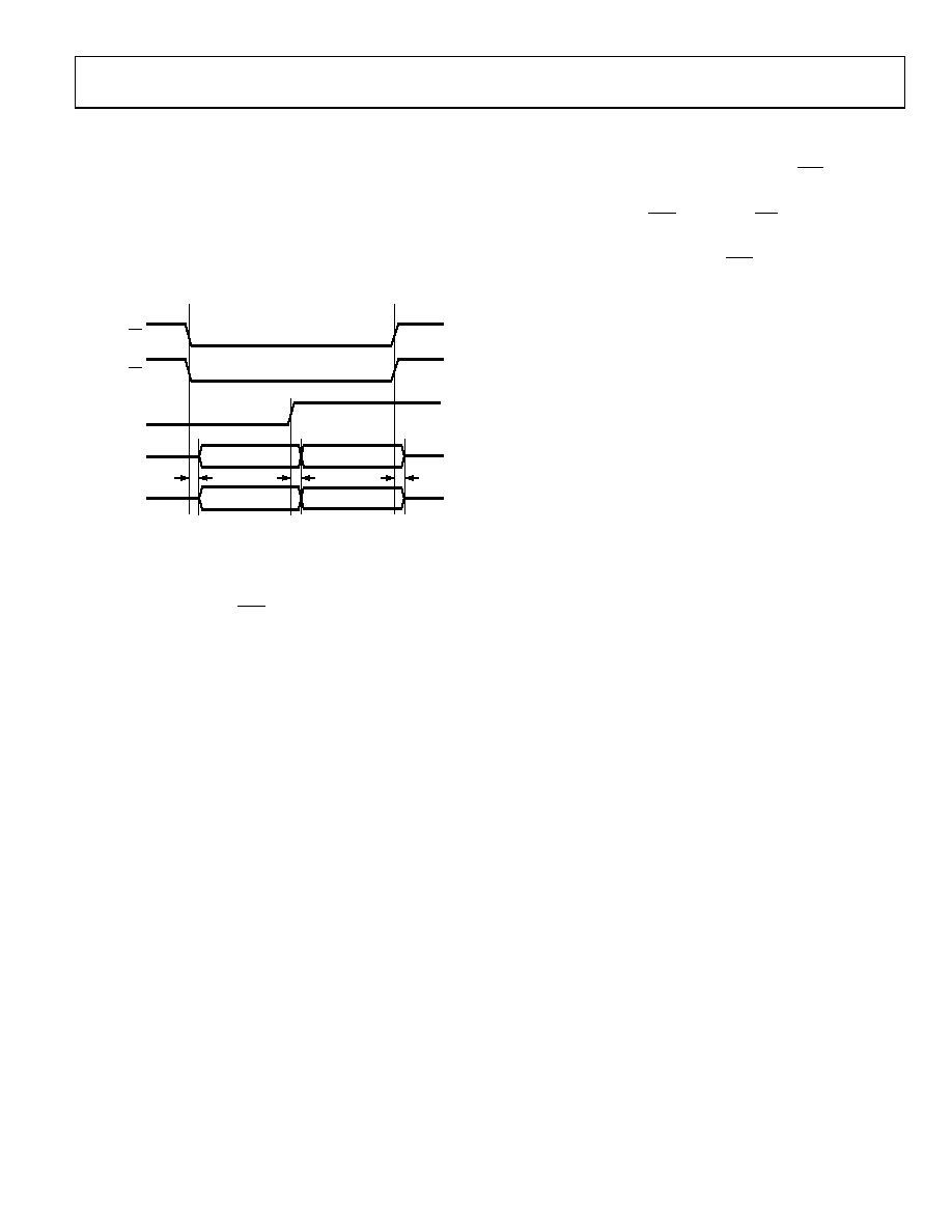
8-Bit Interface (Master or Slave)
The BYTESWAP pin allows a glueless interface to an 8-bit bus.
As shown in Figure 39, when BYTESWAP is low, the LSB byte is
output on D[7:0] and the MSB is output on D[13:8]. When
BYTESWAP is high, the LSB and MSB bytes are swapped; the
LSB is output on D[13:8] and the MSB is output on D[7:0]. By
connecting BYTESWAP to an address line, the 14-bit data can
be read in two bytes on either D[13:8] or D[7:0]. This interface
can be used in both master and slave parallel reading modes.
CS
RD
BYTESWAP
PINS D[13:8]
PINS D[7:0]
HI-Z
HIGH BYTE
LOW BYTE
HIGH BYTE
HI-Z
t12
t13
06
58
9-
0
38
Figure 39. 8-Bit and 14-Bit Parallel Interface
SERIAL INTERFACE
The AD7952 has a serial interface (SPI-compatible) multiplexed
on the data pins D[13:0]. The AD7952 is configured to use the
serial interface when SER/PAR is held high.
Data Interface
The AD7952 outputs 14 bits of data, MSB first, on the SDOUT
pin. This data is synchronized with the 14 clock pulses provided
on the SDCLK pin. The output data is valid on both the rising
and falling edge of the data clock.
Serial Configuration Interface
The AD7952 can be configured through the serial configuration
register only in serial mode, because the serial configuration
pins are also multiplexed on the data pins D[13:10]. See the
Hardware Configuration section and Software Configuration
section for more information.
MASTER SERIAL INTERFACE
The pins multiplexed on D[8:0] and used for master serial
interface are: DIVSCLK[0], DIVSCLK[1], EXT/INT, INVSYNC,
INVSCLK, RDC, SDOUT, SDCLK, and SYNC.
Internal Clock (SER/PAR = High, EXT/INT = Low)
The AD7952 is configured to generate and provide the serial
data clock, SDCLK, when the EXT/INT pin is held low. The
AD7952 also generates a SYNC signal to indicate to the host
when the serial data is valid. The SDCLK and the SYNC signals
can be inverted, if desired, using the INVSCLK and INVSYNC
inputs, respectively. Depending on the input, RDC, the data can
be read during the following conversion or after each conversion.
two modes.
Read During Convert (RDC = High)
Setting RDC = high allows the master read (previous
conversion result) during conversion mode. Usually, because
the AD7952 is used with a fast throughput, this mode is the
most recommended serial mode. In this mode, the serial clock
and data toggle at appropriate instances, minimizing potential
feedthrough between digital activity and critical conversion
decisions. In this mode, the SDCLK period changes because the
LSBs require more time to settle and the SDCLK is derived
from the SAR conversion cycle. In this mode, the AD7952
generates a discontinuous SDCLK of two different periods and
the host should use an SPI interface.
Read After Convert (RDC = Low, DIVSCLK[1:0] = [0 to 3])
Setting RDC = low allows the read after conversion mode.
Unlike the other serial modes, the BUSY signal returns low
after the 14 data bits are pulsed out and not at the end of the
conversion phase, resulting in a longer BUSY width (refer to
Table 4 for BUSY timing specifications). The DIVSCLK[1:0]
inputs control the SDCLK period and SDOUT data rate. As a
result, the maximum throughput cannot be achieved in this
mode. In this mode, the AD7952 also generates a discontinuous
SDCLK; however, a fixed period and hosts supporting both SPI
and serial ports can also be used.
相关PDF资料 |
PDF描述 |
|---|---|
| SP3071EEN-L/TR | IC TXRX RS485/RS422 ESD 8NSOIC |
| AD7492BR-REEL7 | IC ADC 12BIT W/REF W/CLK 24-SOIC |
| ADM101EARMZ-REEL | IC TXRX RS-232 SINGLE 5V 10MSOP |
| VE-B1F-MY | CONVERTER MOD DC/DC 72V 50W |
| VE-B1D-MY | CONVERTER MOD DC/DC 85V 50W |
相关代理商/技术参数 |
参数描述 |
|---|---|
| AD7952BSTZ | 功能描述:IC ADC 14BIT DIFF 1MSPS 48-LQFP RoHS:是 类别:集成电路 (IC) >> 数据采集 - 模数转换器 系列:PulSAR® 其它有关文件:TSA1204 View All Specifications 标准包装:1 系列:- 位数:12 采样率(每秒):20M 数据接口:并联 转换器数目:2 功率耗散(最大):155mW 电压电源:模拟和数字 工作温度:-40°C ~ 85°C 安装类型:表面贴装 封装/外壳:48-TQFP 供应商设备封装:48-TQFP(7x7) 包装:Digi-Reel® 输入数目和类型:4 个单端,单极;2 个差分,单极 产品目录页面:1156 (CN2011-ZH PDF) 其它名称:497-5435-6 |
| AD7952BSTZRL | 功能描述:IC ADC 14BIT DIFF 1MSPS 48-LQFP RoHS:是 类别:集成电路 (IC) >> 数据采集 - 模数转换器 系列:PulSAR® 标准包装:1,000 系列:- 位数:12 采样率(每秒):300k 数据接口:并联 转换器数目:1 功率耗散(最大):75mW 电压电源:单电源 工作温度:0°C ~ 70°C 安装类型:表面贴装 封装/外壳:24-SOIC(0.295",7.50mm 宽) 供应商设备封装:24-SOIC 包装:带卷 (TR) 输入数目和类型:1 个单端,单极;1 个单端,双极 |
| AD795AH | 制造商:未知厂家 制造商全称:未知厂家 功能描述:Voltage-Feedback Operational Amplifier |
| AD795BH | 制造商:未知厂家 制造商全称:未知厂家 功能描述:Voltage-Feedback Operational Amplifier |
| AD795JN | 制造商:Analog Devices 功能描述:Operational Amplifier, Single AMP, Bipolar/JFET, 8 Pin, Plastic, DIP |
发布紧急采购,3分钟左右您将得到回复。