- 您现在的位置:买卖IC网 > PDF目录10657 > AD7982BRMZ (Analog Devices Inc)IC ADC 18BIT 1MSPS PULSAR 10MSOP PDF资料下载
参数资料
| 型号: | AD7982BRMZ |
| 厂商: | Analog Devices Inc |
| 文件页数: | 7/24页 |
| 文件大小: | 0K |
| 描述: | IC ADC 18BIT 1MSPS PULSAR 10MSOP |
| 产品培训模块: | Motor Control |
| 设计资源: | Converting a Single-Ended Signal with AD7982 Differential PulSAR ADC (CN0032) Precision Single-Supply Differential ADC Driver for Industrial-Level Signals (CN0180) |
| 标准包装: | 1 |
| 系列: | PulSAR® |
| 位数: | 18 |
| 采样率(每秒): | 1M |
| 数据接口: | DSP,MICROWIRE?,QSPI?,串行,SPI? |
| 转换器数目: | 1 |
| 功率耗散(最大): | 8.6mW |
| 电压电源: | 单电源 |
| 工作温度: | -40°C ~ 85°C |
| 安装类型: | 表面贴装 |
| 封装/外壳: | 10-TFSOP,10-MSOP(0.118",3.00mm 宽) |
| 供应商设备封装: | 10-MSOP |
| 包装: | 管件 |
| 输入数目和类型: | 1 个差分,单极 |
| 产品目录页面: | 780 (CN2011-ZH PDF) |
Data Sheet
AD7982
Rev. B | Page 15 of 24
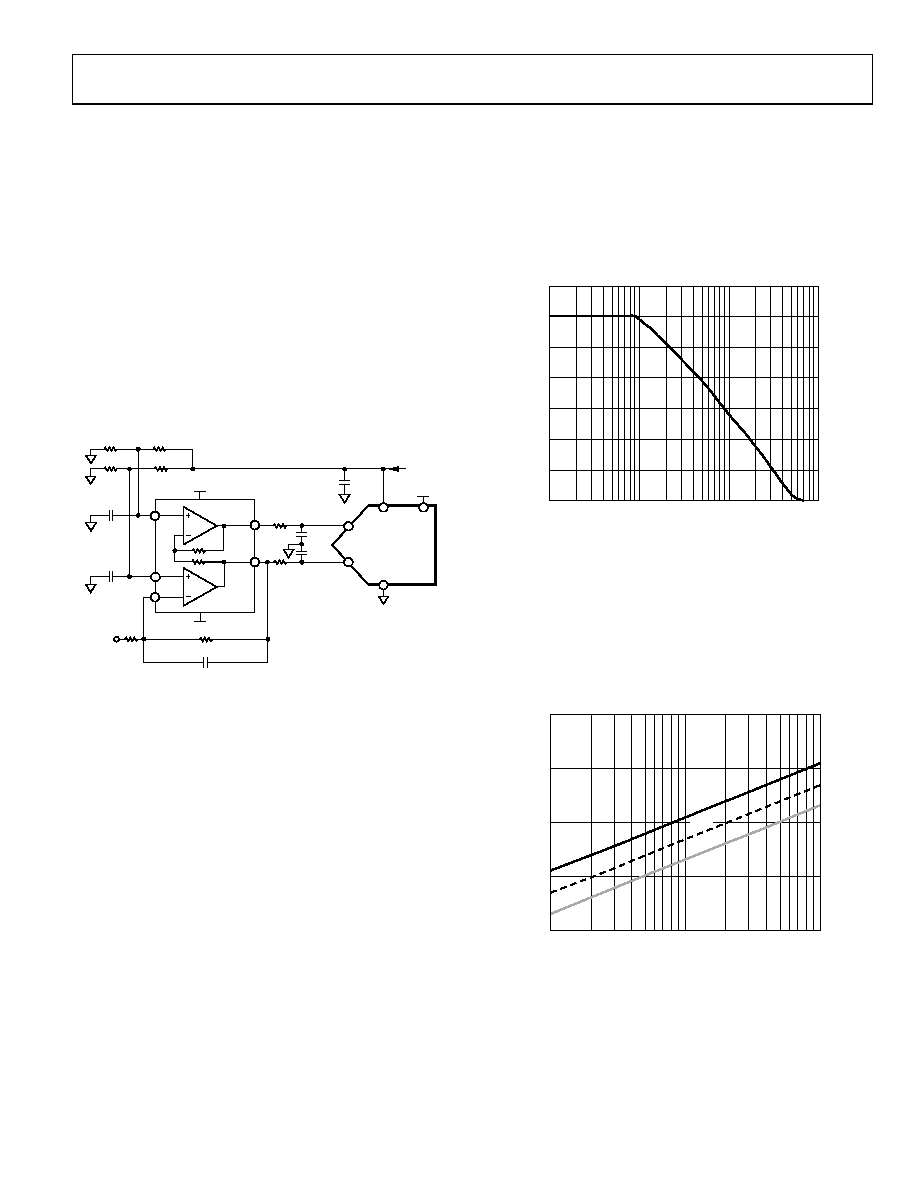
SINGLE-TO-DIFFERENTIAL DRIVER
For applications using a single-ended analog signal, either
bipolar or unipolar, the ADA4941 single-ended-to-differential
driver allows for a differential input to the part. The schematic
is shown in Figure 26.
R1 and R2 set the attenuation ratio between the input range and
the ADC range (VREF). R1, R2, and CF are chosen depending on
the desired input resistance, signal bandwidth, antialiasing, and
noise contribution. For example, for the ±10 V range with a 4 kΩ
impedance, R2 = 1 kΩ and R1 = 4 kΩ.
R3 and R4 set the common mode on the IN input, and R5 and R6
set the common mode on the IN+ input of the ADC. The common
mode should be close to VREF/2. For example, for the ±10 V range
with a single supply, R3 = 8.45 kΩ, R4 = 11.8 kΩ, R5 = 10.5 kΩ,
and R6 = 9.76 kΩ.
06
51
3-
0
15
20
10F
R1
100nF
+2.5V
+5V REF
+5.2V
–0.2V
CF
R2
R4
R6
±10V,
±5V, ..
R3
R5
REF
VDD
GND
IN+
IN–
AD7982
2.7nF
ADA4941
IN
FB
OUTP
OUTN
REF
100nF
Figure 26. Single-Ended-to-Differential Driver Circuit
VOLTAGE REFERENCE INPUT
The AD7982 voltage reference input, REF, has a dynamic input
impedance and should therefore be driven by a low impedance
source with efficient decoupling between the REF and GND
pins, as explained in the Layout section.
When REF is driven by a very low impedance source (for
example, a reference buffer using the AD8031 or the AD8605),
a 10 μF (X5R, 0805 size) ceramic chip capacitor is appropriate
for optimum performance.
If an unbuffered reference voltage is used, the decoupling value
depends on the reference used. For instance, a 22 μF (X5R,
1206 size) ceramic chip capacitor is appropriate for optimum
performance using a low temperature drift ADR43x reference.
If desired, a reference decoupling capacitor with values as small
as 2.2 μF can be used with a minimal impact on performance,
especially DNL.
Regardless, there is no need for an additional lower value ceramic
decoupling capacitor (for example, 100 nF) between the REF
and GND pins.
POWER SUPPLY
The AD7982 uses two power supply pins: a core supply (VDD) and
a digital input/output interface supply (VIO). VIO allows direct
interface with any logic between 1.8 V and 5.5 V. To reduce the
number of supplies needed, VIO and VDD can be tied together.
The AD7982 is independent of power supply sequencing between
VIO and VDD. Additionally, it is very insensitive to power supply
variations over a wide frequency range, as shown in Figure 27.
95
90
85
80
75
70
65
60
P
S
R
(
d
B)
1
10
100
1000
FREQUENCY (kHz)
06
51
3-
0
39
Figure 27. PSRR vs. Frequency
To ensure optimum performance, VDD should be roughly half
of REF, the voltage reference input. For example, if REF is 5.0 V,
VDD should be set to 2.5 V (±5%).
The AD7982 powers down automatically at the end of each
conversion phase; therefore, the power scales linearly with the
sampling rate. This makes the part ideal for low sampling rates
(even of a few hertz) and low battery-powered applications.
0
651
3-
0
37
10.000
1.000
0.100
0.010
0.001
OP
E
R
A
T
ING
C
URRE
NT
S
(m
A)
100000
SAMPLING RATE (SPS)
10000
1000000
IVDD
IVIO
IREF
Figure 28. Operating Currents vs. Sampling Rate
相关PDF资料 |
PDF描述 |
|---|---|
| VI-21R-IW-F4 | CONVERTER MOD DC/DC 7.5V 100W |
| VI-21R-IW-F3 | CONVERTER MOD DC/DC 7.5V 100W |
| LTC1605IN#PBF | IC A/D CONV 16BIT SAMPLNG 28-DIP |
| VI-J1J-MW-F2 | CONVERTER MOD DC/DC 36V 100W |
| VI-21R-IW-F2 | CONVERTER MOD DC/DC 7.5V 100W |
相关代理商/技术参数 |
参数描述 |
|---|---|
| AD7982BRMZRL7 | 功能描述:IC ADC 18BIT 7.0MW 1MSPS 10-MSOP RoHS:是 类别:集成电路 (IC) >> 数据采集 - 模数转换器 系列:PulSAR® 标准包装:1 系列:- 位数:14 采样率(每秒):83k 数据接口:串行,并联 转换器数目:1 功率耗散(最大):95mW 电压电源:双 ± 工作温度:0°C ~ 70°C 安装类型:通孔 封装/外壳:28-DIP(0.600",15.24mm) 供应商设备封装:28-PDIP 包装:管件 输入数目和类型:1 个单端,双极 |
| AD7983 | 制造商:AD 制造商全称:Analog Devices 功能描述:16-Bit, 1.33 MSPS PulSAR ADC in MSOP/QFN |
| AD79831 | 制造商:AD 制造商全称:Analog Devices 功能描述:18-Bit, 2 MSPS PulSAR 15 mW ADC in LFCSP (QFN) |
| AD7983BCPZ-R2 | 功能描述:IC ADC 16BIT 1.33MSPS 10LFCSP 制造商:analog devices inc. 系列:* 包装:带卷(TR) 零件状态:Digi-Key 停止供應 封装/外壳:10-WFDFN 裸露焊盘,CSP 供应商器件封装:10-LFCSP-WD(3x3) 标准包装:250 |
| AD7983BCPZ-RL | 功能描述:IC ADC 16BIT 1.33MSPS 10LFCSP RoHS:是 类别:集成电路 (IC) >> 数据采集 - 模数转换器 系列:PulSAR® 标准包装:1 系列:- 位数:14 采样率(每秒):83k 数据接口:串行,并联 转换器数目:1 功率耗散(最大):95mW 电压电源:双 ± 工作温度:0°C ~ 70°C 安装类型:通孔 封装/外壳:28-DIP(0.600",15.24mm) 供应商设备封装:28-PDIP 包装:管件 输入数目和类型:1 个单端,双极 |
发布紧急采购,3分钟左右您将得到回复。