参数资料
| 型号: | AD8011ANZ |
| 厂商: | Analog Devices Inc |
| 文件页数: | 2/17页 |
| 文件大小: | 0K |
| 描述: | IC OPAMP CF LP LDIST 30MA 8DIP |
| 标准包装: | 50 |
| 放大器类型: | 电流反馈 |
| 电路数: | 1 |
| 转换速率: | 3500 V/µs |
| -3db带宽: | 400MHz |
| 电流 - 输入偏压: | 5µA |
| 电压 - 输入偏移: | 2000µV |
| 电流 - 电源: | 1.3mA |
| 电流 - 输出 / 通道: | 30mA |
| 电压 - 电源,单路/双路(±): | 3 V ~ 12 V,±1.5 V ~ 6 V |
| 工作温度: | -40°C ~ 85°C |
| 安装类型: | 通孔 |
| 封装/外壳: | 8-DIP(0.300",7.62mm) |
| 供应商设备封装: | 8-PDIP |
| 包装: | 管件 |
| 产品目录页面: | 769 (CN2011-ZH PDF) |
REV. C
AD8011
–9–
THEORY OF OPERATION
The AD8011 is a revolutionary generic high speed CF amplifier
that attains new levels of BW, power, distortion, and signal swing
capability. If these key parameters were combined as a figure of
ac merit performance or [(frequency
VSIG)/(distortion
power)],
no IC amplifier today would come close to the merit value of the
AD8011 for frequencies above a few MHz. Its wide dynamic
performance (including noise) is the result of both a new com-
plementary high speed bipolar process and a new and unique
architectural design. The AD8011 uses basically a two gain stage
complementary design approach versus the traditional “single
stage” complementary mirror structure sometimes referred to as
the Nelson amplifier. Though twin stages have been tried before,
they typically consumed high power since they were of a folded
cascade design much like the AD9617. This design allows for
the standing or quiescent current to add to the high signal or slew
current induced stages much like the Nelson or single-stage design.
Thus, in the time domain, the large signal output rise/fall time
and slew rate is controlled typically by the small signal BW of the
amplifier and the input signal step amplitude respectively, not the
dc quiescent current of the gain stages (with the exception of
input level shift diodes Q1/Q2). Using two stages versus one also
allows for a higher overall gain bandwidth product (GBWP) for
the same power, thus lower signal distortion and the ability to
drive heavier external loads. In addition, the second gain stage
also isolates (divides down) A3’s input reflected load drive and
the nonlinearities created resulting in relatively lower distortion
and higher open-loop gain.
Overall, when high external load drive and low ac distortion is a
requirement, a twin gain stage integrating amplifier like the AD8011
will provide superior results for lower power over the traditional
single-stage complementary devices. In addition, being a CF
amplifier, closed-loop BW variations versus external gain variations
(varying RN) will be much lower compared to a VF op amp, where
the BW varies inversely with gain. Another key attribute of this
amplifier is its ability to run on a single 5 V supply due in part to
its wide common-mode input and output voltage range capability.
For 5 V supply operation, the device obviously consumes half
the quiescent power (versus 10 V supply) with little degradation
in its ac and dc performance characteristics. See Specifications.
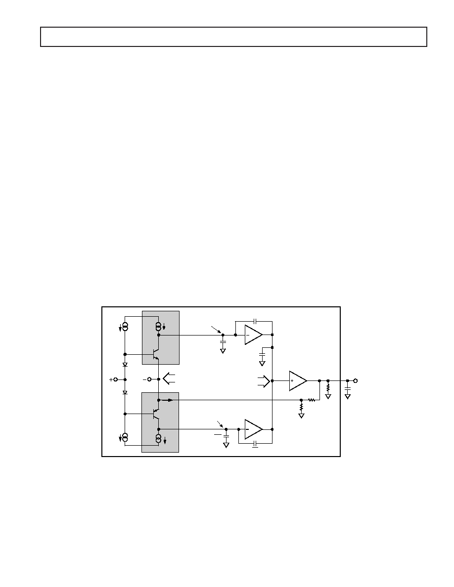
DC GAIN CHARACTERISTICS
Gain stages A1/A1B and A2/A2B combined provide negative
feedforward transresistance gain (see Figure 6). Stage A3 is a unity
gain buffer that provides external load isolation to A2. Each stage
uses a symmetrical complementary design. (A3 is also complemen-
tary though not explicitly shown.) This is done to reduce second
order signal distortion and overall quiescent power as discussed
previously. In the quasi dc to low frequency region, the closed-
loop gain relationship can be approximated as
G = 1 + RF/RN
noninverting operation
G = –RF/RN
inverting operation
These basic relationships are common to all traditional opera-
tional amplifiers. Due to the inverting input error current (IE)
required to servo the output and the inverting IE
RI drop
VP
Q1
Q2
IPP
IPN
VN
ZI
IQ1
Q3
Q4
IE
IR – IFC
IR + IFC
CP1
Z2
A2
CL
RL
ICQ – IO
RF
VO
CD
ICQ + IO
–VI
VO
IQ1
AD8011
A2
CP2
Z1
Z1 = R1 || C1
Z1
CD
RL
A1
INP
A3
Figure 6. Simplified Block Diagram
相关PDF资料 |
PDF描述 |
|---|---|
| AD8011ARZ | IC OPAMP CF LP LDIST 30MA 8SOIC |
| LTC2051HVCDD#PBF | IC OP AMP ZERO-DRIFT DUAL 8-DFN |
| LT1638IDD#PBF | IC OP AMP 1.2MHZ R-R IN/OUT 8DFN |
| LTC2051HVHS8#PBF | IC OP-AMP ZERO-DRIFT DUAL 8-SOIC |
| 929836-01-09-RK | CONN HEADER 18POS DUAL .100 TIN |
相关代理商/技术参数 |
参数描述 |
|---|---|
| AD8011AR | 功能描述:IC OPAMP CF LP LDIST 30MA 8SOIC RoHS:否 类别:集成电路 (IC) >> Linear - Amplifiers - Instrumentation 系列:- 标准包装:50 系列:- 放大器类型:J-FET 电路数:2 输出类型:- 转换速率:13 V/µs 增益带宽积:3MHz -3db带宽:- 电流 - 输入偏压:65pA 电压 - 输入偏移:3000µV 电流 - 电源:1.4mA 电流 - 输出 / 通道:- 电压 - 电源,单路/双路(±):7 V ~ 36 V,±3.5 V ~ 18 V 工作温度:-40°C ~ 85°C 安装类型:通孔 封装/外壳:8-DIP(0.300",7.62mm) 供应商设备封装:8-PDIP 包装:管件 |
| AD8011AR-EBZ | 功能描述:BOARD EVAL FOR AD8011AR RoHS:是 类别:编程器,开发系统 >> 评估板 - 运算放大器 系列:- 产品培训模块:Lead (SnPb) Finish for COTS Obsolescence Mitigation Program 标准包装:1 系列:- |
| AD8011AR-REEL | 制造商:Analog Devices 功能描述:OP Amp Single Current Fdbk ±6V/12V 8-Pin SOIC N T/R |
| AD8011AR-REEL7 | 功能描述:IC OPAMP CF LP LDIST 30MA 8SOIC RoHS:否 类别:集成电路 (IC) >> Linear - Amplifiers - Instrumentation 系列:- 标准包装:2,500 系列:- 放大器类型:通用 电路数:1 输出类型:满摆幅 转换速率:0.11 V/µs 增益带宽积:350kHz -3db带宽:- 电流 - 输入偏压:4nA 电压 - 输入偏移:20µV 电流 - 电源:260µA 电流 - 输出 / 通道:20mA 电压 - 电源,单路/双路(±):2.7 V ~ 36 V,±1.35 V ~ 18 V 工作温度:-40°C ~ 85°C 安装类型:表面贴装 封装/外壳:8-SOIC(0.154",3.90mm 宽) 供应商设备封装:8-SO 包装:带卷 (TR) |
| AD8011ARZ | 功能描述:IC OPAMP CF LP LDIST 30MA 8SOIC RoHS:是 类别:集成电路 (IC) >> Linear - Amplifiers - Instrumentation 系列:- 标准包装:2,500 系列:- 放大器类型:通用 电路数:4 输出类型:- 转换速率:0.6 V/µs 增益带宽积:1MHz -3db带宽:- 电流 - 输入偏压:45nA 电压 - 输入偏移:2000µV 电流 - 电源:1.4mA 电流 - 输出 / 通道:40mA 电压 - 电源,单路/双路(±):3 V ~ 32 V,±1.5 V ~ 16 V 工作温度:0°C ~ 70°C 安装类型:表面贴装 封装/外壳:14-TSSOP(0.173",4.40mm 宽) 供应商设备封装:14-TSSOP 包装:带卷 (TR) 其它名称:LM324ADTBR2G-NDLM324ADTBR2GOSTR |
发布紧急采购,3分钟左右您将得到回复。