参数资料
| 型号: | AD8011ANZ |
| 厂商: | Analog Devices Inc |
| 文件页数: | 3/17页 |
| 文件大小: | 0K |
| 描述: | IC OPAMP CF LP LDIST 30MA 8DIP |
| 标准包装: | 50 |
| 放大器类型: | 电流反馈 |
| 电路数: | 1 |
| 转换速率: | 3500 V/µs |
| -3db带宽: | 400MHz |
| 电流 - 输入偏压: | 5µA |
| 电压 - 输入偏移: | 2000µV |
| 电流 - 电源: | 1.3mA |
| 电流 - 输出 / 通道: | 30mA |
| 电压 - 电源,单路/双路(±): | 3 V ~ 12 V,±1.5 V ~ 6 V |
| 工作温度: | -40°C ~ 85°C |
| 安装类型: | 通孔 |
| 封装/外壳: | 8-DIP(0.300",7.62mm) |
| 供应商设备封装: | 8-PDIP |
| 包装: | 管件 |
| 产品目录页面: | 769 (CN2011-ZH PDF) |
REV. C
–10–
AD8011
(error current times the open-loop inverting input resistance) that
results (see Figure 7), a more exact low frequency closed-loop
transfer function can be described as
A
G
GR
T
R
T
G
A
R
T
V
I
O
F
OO
F
O
=
+
×
+
=
++
11
for noninverting (G is positive).
A
V
O
F
O
G
A
R
T
=
++
1
1 –
for inverting (G is negative).
where G is the ideal gain as previously described. With RI = TO /AO
(open-loop inverting input resistance), the second expression
(positive G) clearly relates to the classical voltage feedback op amp
equation with TO omitted due to its relatively much higher value
and thus insignificant effect. AO and TO are the open-loop dc
voltage and transresistance gains of the amplifier, respectively.
These key transfer variables can be described as
A
Rgmf
A
g
mc
R
O
=
××
×
12
1
|
( –
)
and
T
RA
O
=
×
12
2
|
Therefore
R
g
mc
R
g
mf
I
=
×
1
2
–
where gmc is the positive feedback transconductance (not shown)
and 1/gmf is the thermal emitter resistance of devices D1/D2 and
Q3/Q4. The gmc
× R1 product has a design value that results in a
negative dc open-loop gain of typically –2500 V/V (see Figure 8).
RS
LN
TO (s)
AO (s)
VP
ZI
IE
LI
RN
CP
RF
+VS
–VS
LS
RL
CL
VO
LS
Z I = OPEN LOOP INPUT IMPEDANCE = CI || RL
Figure 7. ZI = Open-Loop Input Impedance
Though atypical of conventional CF or VF amps, this negative
open-loop voltage gain results in an input referred error term
(VP–VO/G = G/AO + RF/TO) that will typically be negative for G,
greater than +3/–4. As an example, for G = 10, AO = –2500,
and TO = 1.2 M
, results in an error of –3 mV using the A
V
derivation above.
This analysis assumes perfect current sources and infinite transistor
VAs. (Q3, Q4 output conductances are assumed zero.) These
assumptions result in actual versus model open-loop voltage gain
and associated input referred error terms being less accurate for
low gain (G) noninverting operation at the frequencies below the
open-loop pole of the AD8011. This is primarily a result of the
input signal (VP) modulating the output conductances of Q3/Q4,
resulting in RI less negative than derived here. For inverting
operation, the actual versus model dc error terms are relatively
much less.
1E+03
1E+04
1E+05
1E+06
1E+07
1E+08
1E+09
80
70
60
50
40
20
10
FREQUENCY (Hz)
30
GAIN
(dB
)
–90
PHASE
(Degrees)
–100
–110
–120
–160
PHASE
GAIN
0
–10
–20
–30
–170
–180
–190
–200
–130
–140
–150
AO(s)
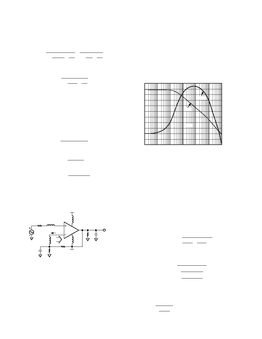
Figure 8. Open-Loop Voltage Gain and Phase
AC TRANSFER CHARACTERISTICS
The ac small signal transfer derivations below are based on a
simplified single-pole model. Though inaccurate at frequencies
approaching the closed-loop BW (CLBW) of the AD8011 at low
noninverting external gains, they still provide a fair approxima-
tion and an intuitive understanding of its primary ac small signal
characteristics.
For inverting operation and high noninverting gains, these
transfer equations provide a good approximation to the actual
ac performance of the device.
To accurately quantify the VO versus VP relationship, AO(s)
and TO(s) need to be derived. This can be seen by the following
nonexpanded noninverting gain relationship
Vs
V s
G
As
R
Ts
OP
O
F
O
() /
()
[]
=
++ 1
with
As
Rg
mf
A
g
mc
R
S
g
mc
R
O ()
||
–
=
××
×
12
11
1
11
τ
where R1 is the input resistance to A2/A2B, and
τ1 (equal to
CD
R1
A2) is the open-loop dominate time constant,
and
T
s
AR
s
O ()
||
=
×
+
21
2
11
τ
相关PDF资料 |
PDF描述 |
|---|---|
| AD8011ARZ | IC OPAMP CF LP LDIST 30MA 8SOIC |
| LTC2051HVCDD#PBF | IC OP AMP ZERO-DRIFT DUAL 8-DFN |
| LT1638IDD#PBF | IC OP AMP 1.2MHZ R-R IN/OUT 8DFN |
| LTC2051HVHS8#PBF | IC OP-AMP ZERO-DRIFT DUAL 8-SOIC |
| 929836-01-09-RK | CONN HEADER 18POS DUAL .100 TIN |
相关代理商/技术参数 |
参数描述 |
|---|---|
| AD8011AR | 功能描述:IC OPAMP CF LP LDIST 30MA 8SOIC RoHS:否 类别:集成电路 (IC) >> Linear - Amplifiers - Instrumentation 系列:- 标准包装:50 系列:- 放大器类型:J-FET 电路数:2 输出类型:- 转换速率:13 V/µs 增益带宽积:3MHz -3db带宽:- 电流 - 输入偏压:65pA 电压 - 输入偏移:3000µV 电流 - 电源:1.4mA 电流 - 输出 / 通道:- 电压 - 电源,单路/双路(±):7 V ~ 36 V,±3.5 V ~ 18 V 工作温度:-40°C ~ 85°C 安装类型:通孔 封装/外壳:8-DIP(0.300",7.62mm) 供应商设备封装:8-PDIP 包装:管件 |
| AD8011AR-EBZ | 功能描述:BOARD EVAL FOR AD8011AR RoHS:是 类别:编程器,开发系统 >> 评估板 - 运算放大器 系列:- 产品培训模块:Lead (SnPb) Finish for COTS Obsolescence Mitigation Program 标准包装:1 系列:- |
| AD8011AR-REEL | 制造商:Analog Devices 功能描述:OP Amp Single Current Fdbk ±6V/12V 8-Pin SOIC N T/R |
| AD8011AR-REEL7 | 功能描述:IC OPAMP CF LP LDIST 30MA 8SOIC RoHS:否 类别:集成电路 (IC) >> Linear - Amplifiers - Instrumentation 系列:- 标准包装:2,500 系列:- 放大器类型:通用 电路数:1 输出类型:满摆幅 转换速率:0.11 V/µs 增益带宽积:350kHz -3db带宽:- 电流 - 输入偏压:4nA 电压 - 输入偏移:20µV 电流 - 电源:260µA 电流 - 输出 / 通道:20mA 电压 - 电源,单路/双路(±):2.7 V ~ 36 V,±1.35 V ~ 18 V 工作温度:-40°C ~ 85°C 安装类型:表面贴装 封装/外壳:8-SOIC(0.154",3.90mm 宽) 供应商设备封装:8-SO 包装:带卷 (TR) |
| AD8011ARZ | 功能描述:IC OPAMP CF LP LDIST 30MA 8SOIC RoHS:是 类别:集成电路 (IC) >> Linear - Amplifiers - Instrumentation 系列:- 标准包装:2,500 系列:- 放大器类型:通用 电路数:4 输出类型:- 转换速率:0.6 V/µs 增益带宽积:1MHz -3db带宽:- 电流 - 输入偏压:45nA 电压 - 输入偏移:2000µV 电流 - 电源:1.4mA 电流 - 输出 / 通道:40mA 电压 - 电源,单路/双路(±):3 V ~ 32 V,±1.5 V ~ 16 V 工作温度:0°C ~ 70°C 安装类型:表面贴装 封装/外壳:14-TSSOP(0.173",4.40mm 宽) 供应商设备封装:14-TSSOP 包装:带卷 (TR) 其它名称:LM324ADTBR2G-NDLM324ADTBR2GOSTR |
发布紧急采购,3分钟左右您将得到回复。