- 您现在的位置:买卖IC网 > PDF目录3544 > AD8017ARZ-REEL7 (Analog Devices Inc)IC AMP GP DUAL LP LDIST 8SOIC PDF资料下载
参数资料
| 型号: | AD8017ARZ-REEL7 |
| 厂商: | Analog Devices Inc |
| 文件页数: | 6/17页 |
| 文件大小: | 0K |
| 描述: | IC AMP GP DUAL LP LDIST 8SOIC |
| 标准包装: | 1,000 |
| 放大器类型: | 通用 |
| 电路数: | 2 |
| 转换速率: | 1600 V/µs |
| -3db带宽: | 160MHz |
| 电流 - 输入偏压: | 16µA |
| 电压 - 输入偏移: | 1800µV |
| 电流 - 电源: | 7mA |
| 电流 - 输出 / 通道: | 270mA |
| 电压 - 电源,单路/双路(±): | 4.4 V ~ 12 V,±2.2 V ~ 6 V |
| 工作温度: | -40°C ~ 85°C |
| 安装类型: | 表面贴装 |
| 封装/外壳: | 8-SOIC(0.154",3.90mm 宽) |
| 供应商设备封装: | 8-SOIC |
| 包装: | 带卷 (TR) |
| 配用: | AD8018ARU-EVAL-ND - BOARD EVAL FOR AD8018 AD8018AR-EVAL-ND - BOARD EVAL FOR AD8018 AD8017AR-EVAL-ND - BOARD EVAL FOR AD8017 |
AD8017
–13–
REV. C
The practical maximum value that these resistors can have is
determined by the offset voltage that is created by the input bias
current that flows through them. The maximum input bias
current into the + inputs is 45
A. This will create an offset
voltage of 45 mV per 1 k
of bias resistor. Fortunately, the ac
coupling of the stages provides only unity gain for this dc offset
voltage, which is another advantage of this configuration. Any
dc offset in the output will limit the amount of dynamic signal
swing that will be available between the rails.
The circuit shown uses two 4.7 V Zener diodes that provide a
voltage drop which serves to limit the power dissipation in the
bias circuit. This allows the use of smaller value resistors in the
bias circuit. Thus, for this circuit the current will be (12 V –
(2
× 4.7 V))/2 k = 1.3 mA. Thus, this circuit will dissipate
only 15.6 mW, yet only induce a maximum of 40 mV of offset
at the output. This circuit will also track the midpoint of the
supplies over their specified tolerance range.
The distortion of the circuit was measured with a 50
load.
The frequency used was 500 kHz, which is beyond the maxi-
mum required for the upstream signal. For ADSL over POTS,
a maximum frequency of 135 kHz is required. For ADSL over
ISDN, the maximum frequency is 276 kHz. The amplitude was
20 V p-p (10 V p-p for each amplifier), which is the maximum
crest signal that will be required. The second harmonic was better
than –80 dBc, while the third harmonic was –64 dBc. This
represents a worst case of the absolute maximum signal that will
be required for only a very small statistical basis and at a fre-
quency that is higher than the maximum required. For a statisti-
cal majority of the time, the signal will be at a lower amplitude
and frequency, where the distortion performance will be better.
When the circuit was run while providing the upstream drive signal
in an ADSL system, the supply current to the part was mea-
sured at 25 mA. Thus, the total power to the drive circuit was
300 mW. This power winds up in three places: the drive ampli-
fier, down the line and in the termination and interface circuitry.
The ADSL specification calls for 13 dBm or 20 mW into the line.
The line termination will consume an equal amount of power, as
it is the same resistance value. About a 1 dB loss can be expected
in the losses in the interface circuitry, which translates into about
10 mW of power. Thus, the total power dissipated in the AD8017
when used as a driver in this application is about 250 mW.
A1
RL
VO1
VO2
VCC
VEE
Figure 8. Differential Driver Simplified Circuit Schematic
It is important to consider the total power dissipation of the
AD8017 in order to properly size the heat sinking area for your
application. The dc power dissipation for VIN = 0 is simply,
IQ. (VCC + VEE), or 2
× I
Q
× V
S. For the AD8017, this number is
0.17 W. In this purely differential circuit we can use symmetry
to simplify the computation for a dc input signal,
PI
V
R
DQ
S
O
L
=×
×
+ ×
()×
24
–
This formula is slightly pessimistic due to the fact that some of
the quiescent supply current commutates during sourcing or
sinking current into the load. For a sine wave source, integration
over a half cycle yields:
PI
V
VV
R
V
R
DQ
S
OS
L
O
L
=×
×
+ ×
22
4
2
π
(Refer to Figure 41)
The situation is more complicated with a complex modulated
signal. In the case of a DMT signal, taking the equivalent sine wave
power overestimates the power dissipation by > 15%. For example:
POUT = 16 dBm = 40 mW
VOUT @ 50
= 1.41 V rms or V
O = 1.0 V
at each amplifier output, which yields a PD of 0.436 W. By
actual measurement, PD for a DMT signal of 16 dBm requires
0.38 W of power to be dissipated by the AD8017.
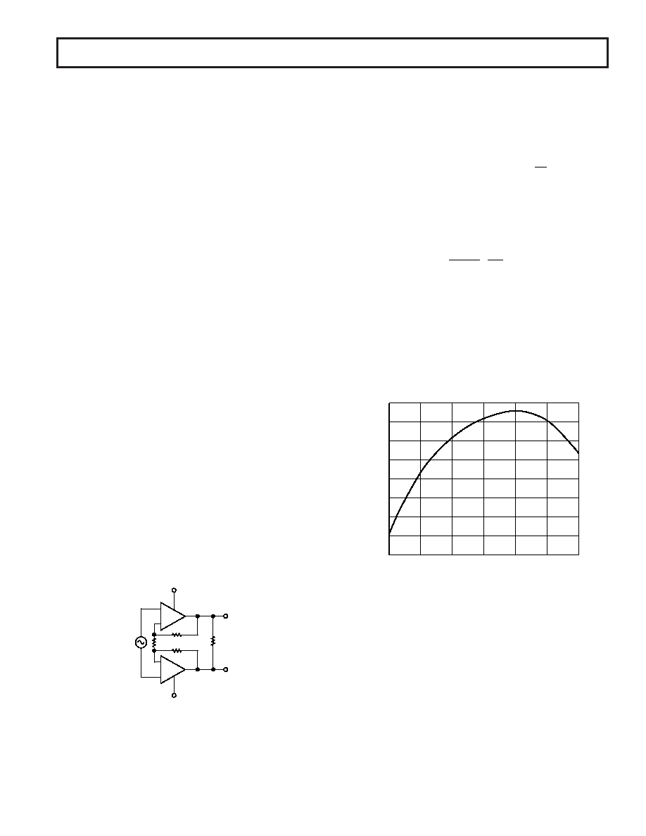
OUTPUT VOLTAGE (VO) – VPK
POWER
DISSIPATION
(P
D
)
–
W
0.8
0
0.2
4
12
03
0.3
0.4
0.5
0.6
0.7
0.1
56
Figure 9. Power Dissipation (PD) vs. Output Voltage (VO),
RL = 50
Thermal Considerations
The AD8017 in a “Thermal Coastline” SO-8 package relies on
the device pins to assist in removing heat from the die at a faster
rate than that of conventional packages. The effect is to provide
a lower
θJC for the device. To make the most effective use of
this, special details should be worked into the copper traces of
the printed circuit board.
There will be a tradeoff, however, between designing a board
that will maximally remove heat, and one that will provide the
desired ac performance. This is the result of the additional para-
sitic capacitance on some of the pins that would be caused by
the addition of extra heat sinking copper traces.
相关PDF资料 |
PDF描述 |
|---|---|
| MAX4073FAXK+T | IC AMP CURRENT SENSE SC70-5 |
| RC0805FR-0771K5L | RES 71.5K OHM 1/8W 1% 0805 SMD |
| AS168X-CB3G200 | CIRCUIT BRKR THERMAL 20.0A 3POLE |
| 87465-1 | 08 MODII HDR SRST UNSHRD .100 |
| AS168X-CB3G320 | CIRCUIT BRKR THERMAL 32.0A 3POLE |
相关代理商/技术参数 |
参数描述 |
|---|---|
| AD8018 | 制造商:AD 制造商全称:Analog Devices 功能描述:5 V, Rail-to-Rail, High-Output Current, xDSL Line Drive Amplifier |
| AD80182ABSVZ | 制造商:Analog Devices 功能描述: |
| AD80182BSVZ | 制造商:Analog Devices 功能描述: |
| AD80184BBCZ | 制造商:Analog Devices 功能描述: |
| AD80185BBCZ | 制造商:Analog Devices 功能描述: |
发布紧急采购,3分钟左右您将得到回复。