- 您现在的位置:买卖IC网 > PDF目录3544 > AD8017ARZ-REEL7 (Analog Devices Inc)IC AMP GP DUAL LP LDIST 8SOIC PDF资料下载
参数资料
| 型号: | AD8017ARZ-REEL7 |
| 厂商: | Analog Devices Inc |
| 文件页数: | 7/17页 |
| 文件大小: | 0K |
| 描述: | IC AMP GP DUAL LP LDIST 8SOIC |
| 标准包装: | 1,000 |
| 放大器类型: | 通用 |
| 电路数: | 2 |
| 转换速率: | 1600 V/µs |
| -3db带宽: | 160MHz |
| 电流 - 输入偏压: | 16µA |
| 电压 - 输入偏移: | 1800µV |
| 电流 - 电源: | 7mA |
| 电流 - 输出 / 通道: | 270mA |
| 电压 - 电源,单路/双路(±): | 4.4 V ~ 12 V,±2.2 V ~ 6 V |
| 工作温度: | -40°C ~ 85°C |
| 安装类型: | 表面贴装 |
| 封装/外壳: | 8-SOIC(0.154",3.90mm 宽) |
| 供应商设备封装: | 8-SOIC |
| 包装: | 带卷 (TR) |
| 配用: | AD8018ARU-EVAL-ND - BOARD EVAL FOR AD8018 AD8018AR-EVAL-ND - BOARD EVAL FOR AD8018 AD8017AR-EVAL-ND - BOARD EVAL FOR AD8017 |
AD8017
–14–
REV. C
The first technique for maximum heat sinking is to use a heavy
layer of copper. 2 oz. copper will provide better heat sinking
than 1 oz. copper. Additional internal circuit layers can also be
used to more effectively remove heat, and to provide better
power and ground distribution.
There are no “ground” pins per se on the AD8017 (when run
on a dual supply), but the power supplies (Pins 4 and 8) are at
ac ground. Thus, these pins can be safely tied to a maximum
area of copper foil without affecting the ac performance of the
part. On the surface side of the board, the copper area that
connects to Pins 4 and 8 should be enlarged and spread out to
the maximum extent possible. As a practical matter, there will
be diminishing returns from adding copper more than a few
centimeters from the pins.
When the power supplies are run on the board on internal
power planes, then these should also be made as large as practi-
cal, and multiple vias (~0.012 in. or 0.3 mm) should be provided
from the component layer near the power supply pins of the
AD8017 to the inner layers. These vias should not have any of
the traditional “thermal relief” spokes to the planes, because the
function of these is to impede heat flow for ease of soldering.
This is counter to the effect desired for heat sinking.
On the side of the board opposite the component, additional
heat sinking can be provided by adding copper area near the vias
to further lower the thermal resistance. Additional vias can be
provided throughout to better conduct heat from the inner layers
to the outer layers.
The remainder of the device pins are active signal pins and must
be treated a bit more carefully. Pins 2 and 6 are the summing
junctions of the op amps and will be the most adversely affected by
stray capacitance. For this reason, the copper area of these pins
should be minimized. In addition, the copper nearby on the
component layer should be kept more than 3 mm–5 mm away
from these pins, where possible. The inner and opposite side
circuit layers directly below the summing junctions should also
be void of copper.
The positive inputs and outputs can withstand somewhat more
capacitance than the summing junctions without adversely
affecting ac performance. However, these pins should be treated
carefully, and the amount of heat sinking and excess capacitance
should be analyzed and adjusted depending on the application.
If maximum ac performance is desired and the power dissipa-
tion is not extreme, then the copper area connected to these pins
should be minimized. If the ac performance is not very critical
and maximum power must be dissipated, then the copper area
connected to these pins can be increased. As in many other
areas of analog design, the designer must use some judgment
based on the consideration of the above, in order to produce a
satisfactory design.
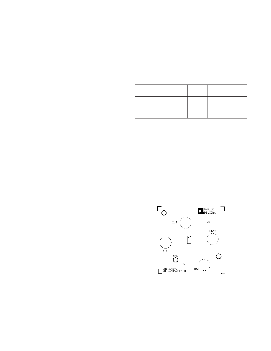
LAYOUT CONSIDERATIONS
The specified high speed performance of the AD8017 requires
careful attention to board layout and component selection.
Table II shows recommended component values for the AD8017
and Figures 10–12 show recommended layouts for the 8-lead
SOIC package for a positive gain. Proper RF design techniques
and low parasitic component selections are mandatory.
Table II. Typical Bandwidth vs. Gain Setting Resistors
(VS = 6 V, RL = 100
)
Small Signal
Gain
RF ( )RG ( )RT ( )
–3 dB BW (MHz)
–1
619
54.5
110
+1
619
49.9
320
+2
619
49.9
160
+10
619
68.8
49.9
40
RT chosen for 50
characteristic input impedance.
The PCB should have a ground plane covering all unused
portions of the component side of the board to provide a low
impedance ground path. The ground plane should be removed
from the area near the input pins to reduce stray capacitance.
Chip capacitors should be used for supply bypassing (see Fig-
ures 4 and 5). One end should be connected to the ground
plane and the other within 1/8 in. of each power pin. An addi-
tional (4.7
F–10 F) tantalum electrolytic capacitor should be
connected in parallel.
The feedback resistor should be located close to the inverting
input pin in order to keep the stray capacitance at this node to
a minimum. Capacitance greater than 1.5 pF at the inverting
input will significantly affect high speed performance when
operating at low noninverting gain.
Figure 10. Universal SOIC Noninverter Top Silkscreen
相关PDF资料 |
PDF描述 |
|---|---|
| MAX4073FAXK+T | IC AMP CURRENT SENSE SC70-5 |
| RC0805FR-0771K5L | RES 71.5K OHM 1/8W 1% 0805 SMD |
| AS168X-CB3G200 | CIRCUIT BRKR THERMAL 20.0A 3POLE |
| 87465-1 | 08 MODII HDR SRST UNSHRD .100 |
| AS168X-CB3G320 | CIRCUIT BRKR THERMAL 32.0A 3POLE |
相关代理商/技术参数 |
参数描述 |
|---|---|
| AD8018 | 制造商:AD 制造商全称:Analog Devices 功能描述:5 V, Rail-to-Rail, High-Output Current, xDSL Line Drive Amplifier |
| AD80182ABSVZ | 制造商:Analog Devices 功能描述: |
| AD80182BSVZ | 制造商:Analog Devices 功能描述: |
| AD80184BBCZ | 制造商:Analog Devices 功能描述: |
| AD80185BBCZ | 制造商:Analog Devices 功能描述: |
发布紧急采购,3分钟左右您将得到回复。