参数资料
| 型号: | AD8030ARZ-REEL7 |
| 厂商: | Analog Devices Inc |
| 文件页数: | 11/25页 |
| 文件大小: | 0K |
| 描述: | IC AMP GP R-R DUAL LP 8SOIC |
| 标准包装: | 1,000 |
| 放大器类型: | 通用 |
| 电路数: | 2 |
| 输出类型: | 满摆幅 |
| 转换速率: | 63 V/µs |
| -3db带宽: | 125MHz |
| 电流 - 输入偏压: | 1.7µA |
| 电压 - 输入偏移: | 2000µV |
| 电流 - 电源: | 1.4mA |
| 电流 - 输出 / 通道: | 170mA |
| 电压 - 电源,单路/双路(±): | 2.7 V ~ 12 V,±1.35 V ~ 6 V |
| 工作温度: | -40°C ~ 125°C |
| 安装类型: | 表面贴装 |
| 封装/外壳: | 8-SOIC(0.154",3.90mm 宽) |
| 供应商设备封装: | 8-SO |
| 包装: | 带卷 (TR) |
AD8029/AD8030/AD8040
Data Sheet
Rev. B | Page 18 of 24
Table 5. Effect of Load on Performance
Noninverting
Gain
RF
(k)
RG
(k)
RLOAD
(k)
–3 dB SS BW
(MHz)
Peaking
(dB)
HD2 at 1 MHz,
2 V p-p (dB)
HD3 at 1 MHz,
2 V p-p (dB)
Output Noise
(nV/√Hz)
1
0
N/A
1
120
0.02
–80
–72
16.5
1
0
N/A
2
130
0.6
–84
–83
16.5
1
0
N/A
5
139
1
–87.5
–92.5
16.5
2
1
36
0
–72
–60
33.5
2
2.5
44.5
0.2
–79
–72.5
34.4
2
5
43
2
–84
–86
36
–1
1
40
0.01
–68
–57
33.6
–1
2.5
40
0.05
–74
–68
34
–1
5
34
1
–78
–80
36
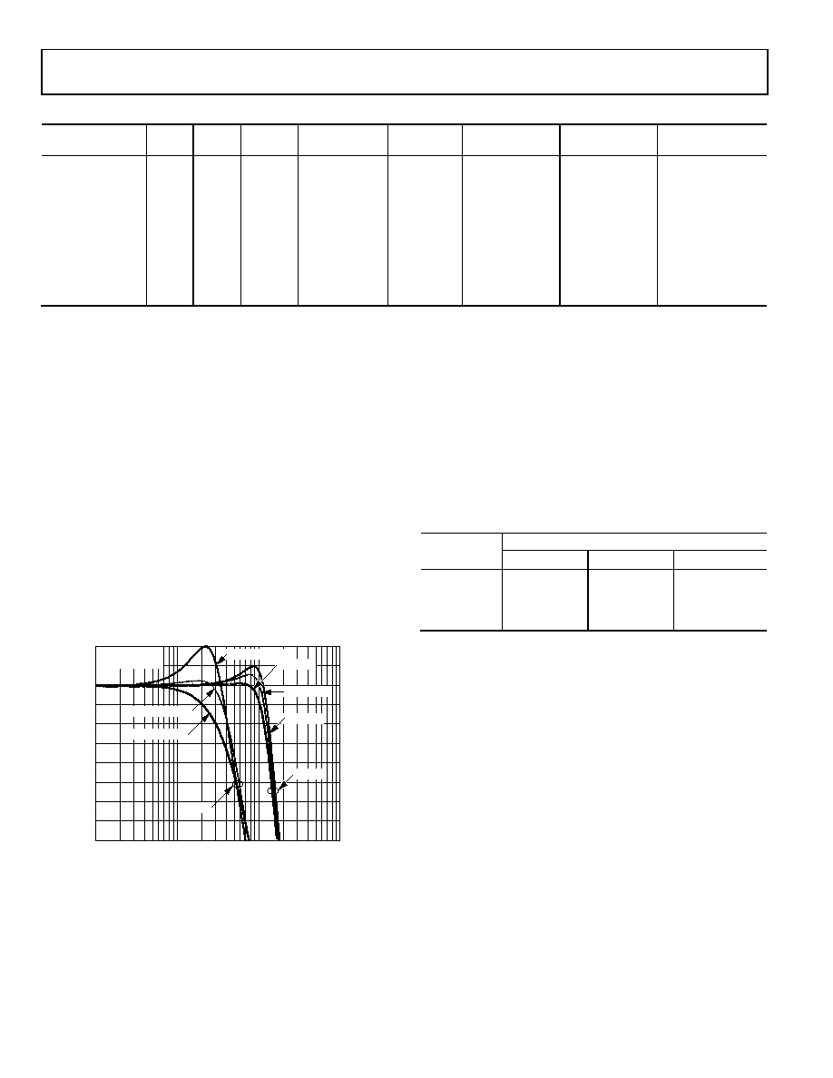
The feedback resistance (RF || RG) combines with the input
capacitance to form a pole in the amplifier’s loop response. This
can cause peaking and ringing in the amplifier’s response if the
RC time constant is too low. Figure 55 illustrates this effect.
Peaking can be reduced by adding a small capacitor (1 pF–4 pF)
across the feedback resistor. The best way to find the optimal
value of capacitor is to empirically try it in your circuit. Another
factor of higher resistance values is the impact it has on noise
performance. Higher resistor values generate more noise. Each
application is unique and therefore a balance must be reached
between distortion, peaking, and noise performance. Table 5
outlines the trade-offs that different loads have on distortion,
peaking, and noise performance. In gains of 1, 2, and 10,
equivalent loads of 1 k, 2 k, and 5 k are shown.
With increasing load resistance, the distortion and –3 dB
bandwidth improve, while the noise and peaking degrade
slightly.
RL = 5k
FREQUENCY (MHz)
NORMALIZED
CLOSED-LOOP
GAIN
(dB)
1
–8
10
100
1000
03679-A-007
2
1
0
–1
–2
–3
–4
–5
–6
RL = 2.5k
–7
RF = RL = 5k
RF = RL = 2.5k
RF = RL = 1k
G = +2
G = +1
RL = 1k
VS = 5V
VOUT = 0.1V p-p
Figure 55. Frequency Response for Various Feedback/Load Resistances
DISABLE PIN
The AD8029 disable pin allows the amplifier to be shut down
for power conservation or multiplexing applications. When in
the disable mode, the amplifier draws only 150 A of quiescent
current. The disable pin control voltage is referenced to the
negative supply. The amplifier enters power-down mode any
time the disable pin is tied to the most negative supply or within
0.8 V of the negative supply. If left open, the amplifier will
operate normally. For switching levels, refer to Table 6.
Table 6. Disable Pin Control Voltage
Disable Pin
Voltage
Supply Voltage
+3 V
+5 V
±5 V
Low
(Disabled)
0 V to <0.8 V
–5 V to <–4 .2 V
High
(Enabled)
1.2 V to 3 V
1.2 V to 5 V
–3.8 V to +5 V
相关PDF资料 |
PDF描述 |
|---|---|
| 0034.5616.22 | FUSE 800MA 250V TLAG 5X20 SMD TR |
| ADA4930-2YCPZ-R2 | IC DIFF AMP 1.35GHZ 24-LFCSP |
| 0034.5617.22 | FUSE 1A 250V T-LAG 5X20 SMD T/R |
| KTR10EZPF1804 | RES 1.80M OHM 1/8W 1% 0805 SMD |
| 0034.5619.22 | FUSE 1.6MA 250V TLAG 5X20 SMD TR |
相关代理商/技术参数 |
参数描述 |
|---|---|
| AD8031 | 制造商:AD 制造商全称:Analog Devices 功能描述:2.7 V, 800 レA, 80 MHz Rail-to-Rail I/O Amplifiers |
| AD8031_06 | 制造商:AD 制造商全称:Analog Devices 功能描述:2.7 V, 800 レA, 80 MHz Rail-to-Rail I/O Amplifiers |
| AD8031A | 制造商:AD 制造商全称:Analog Devices 功能描述:2.7 V, 800 uA, 80 MHz Rail-to-Rail I/O Amplifiers |
| AD8031AN | 制造商:Rochester Electronics LLC 功能描述:PDIP SINGLE LOW POWER OP AMP - Bulk 制造商:Analog Devices 功能描述:IC SM AMP LOW POWER RRI/O |
| AD8031ANZ | 功能描述:IC OPAMP VF R-R LP LDIST 8DIP RoHS:是 类别:集成电路 (IC) >> Linear - Amplifiers - Instrumentation 系列:- 产品培训模块:Differential Circuit Design Techniques for Communication Applications 标准包装:1 系列:- 放大器类型:RF/IF 差分 电路数:1 输出类型:差分 转换速率:9800 V/µs 增益带宽积:- -3db带宽:2.9GHz 电流 - 输入偏压:3µA 电压 - 输入偏移:- 电流 - 电源:40mA 电流 - 输出 / 通道:- 电压 - 电源,单路/双路(±):3 V ~ 3.6 V 工作温度:-40°C ~ 85°C 安装类型:表面贴装 封装/外壳:16-VQFN 裸露焊盘,CSP 供应商设备封装:16-LFCSP-VQ 包装:剪切带 (CT) 产品目录页面:551 (CN2011-ZH PDF) 其它名称:ADL5561ACPZ-R7CT |
发布紧急采购,3分钟左右您将得到回复。