- 您现在的位置:买卖IC网 > PDF目录5369 > ADA4930-2YCPZ-R2 (Analog Devices Inc)IC DIFF AMP 1.35GHZ 24-LFCSP PDF资料下载
参数资料
| 型号: | ADA4930-2YCPZ-R2 |
| 厂商: | Analog Devices Inc |
| 文件页数: | 1/29页 |
| 文件大小: | 0K |
| 描述: | IC DIFF AMP 1.35GHZ 24-LFCSP |
| 标准包装: | 1 |
| 放大器类型: | 差分 |
| 电路数: | 2 |
| 输出类型: | 差分 |
| 转换速率: | 3400 V/µs |
| -3db带宽: | 1.35GHz |
| 电流 - 输入偏压: | 23µA |
| 电压 - 输入偏移: | 150µV |
| 电流 - 电源: | 34mA |
| 电流 - 输出 / 通道: | 30mA |
| 电压 - 电源,单路/双路(±): | 3.3V,5V |
| 工作温度: | -40°C ~ 105°C |
| 安装类型: | 表面贴装 |
| 封装/外壳: | 24-VFQFN 裸露焊盘,CSP |
| 供应商设备封装: | 24-LFCSP-VQ(4x4) |
| 包装: | 标准包装 |
| 其它名称: | ADA4930-2YCPZ-R2DKR |
当前第1页第2页第3页第4页第5页第6页第7页第8页第9页第10页第11页第12页第13页第14页第15页第16页第17页第18页第19页第20页第21页第22页第23页第24页第25页第26页第27页第28页第29页
Ultralow Noise
Drivers for Low Voltage ADCs
ADA4930-1/ADA4930-2
Rev. A
Information furnished by Analog Devices is believed to be accurate and reliable. However, no
responsibilityis assumedbyAnalogDevicesforitsuse,norforanyinfringementsof patentsorother
rightsofthirdpartiesthatmayresultfromitsuse.Specificationssubjecttochangewithoutnotice.No
license is granted by implication or otherwise under any patent or patent rights of Analog Devices.
Trademarksandregisteredtrademarksarethepropertyoftheirrespectiveowners.
One Technology Way, P.O. Box 9106, Norwood, MA 02062-9106, U.S.A.
Tel: 781.329.4700
www.analog.com
Fax: 781.461.3113
2010 Analog Devices, Inc. All rights reserved.
FEATURES
Low input voltage noise: 1.2 nV/√Hz
Low common-mode output: 0.9 V on single supply
Extremely low harmonic distortion
104 dBc HD2 at 10 MHz
79 dBc HD2 at 70 MHz
73 dBc HD2 at 100 MHz
101 dBc HD3 at 10 MHz
82 dBc HD3 at 70 MHz
75 dBc HD3 at 100 MHz
High speed
3 dB bandwidth of 1.35 GHz, G = 1
Slew rate: 3400 V/μs, 25% to 75%
0.1 dB gain flatness to 380 MHz
Fast overdrive recovery of 1.5 ns
0.5 mV typical offset voltage
Externally adjustable gain
Differential-to-differential or single-ended-to-differential
operation
Adjustable output common-mode voltage
Single-supply operation: 3.3 V or 5 V
APPLICATIONS
ADC drivers
Single-ended-to-differential converters
IF and baseband gain blocks
Differential buffers
Line drivers
GENERAL DESCRIPTION
The ADA4930-1/ADA4930-2 are very low noise, low distortion,
high speed differential amplifiers. They are an ideal choice for
driving 1.8 V high performance ADCs with resolutions up to
14 bits from dc to 70 MHz. The adjustable output common
mode allows the ADA4930-1/ADA4930-2 to match the input of
the ADC. The internal common-mode feedback loop provides
exceptional output balance, suppression of even-order harmonic
distortion products, and dc level translation.
With the ADA4930-1/ADA4930-2, differential gain configurations
are easily realized with a simple external feedback network of
four resistors determining the closed-loop gain of the amplifier.
The ADA4930-1/ADA4930-2 are fabricated using Analog Devices,
Inc., proprietary silicon-germanium (SiGe), complementary
bipolar process, enabling them to achieve very low levels of
distortion with an input voltage noise of only 1.2 nV/√Hz.
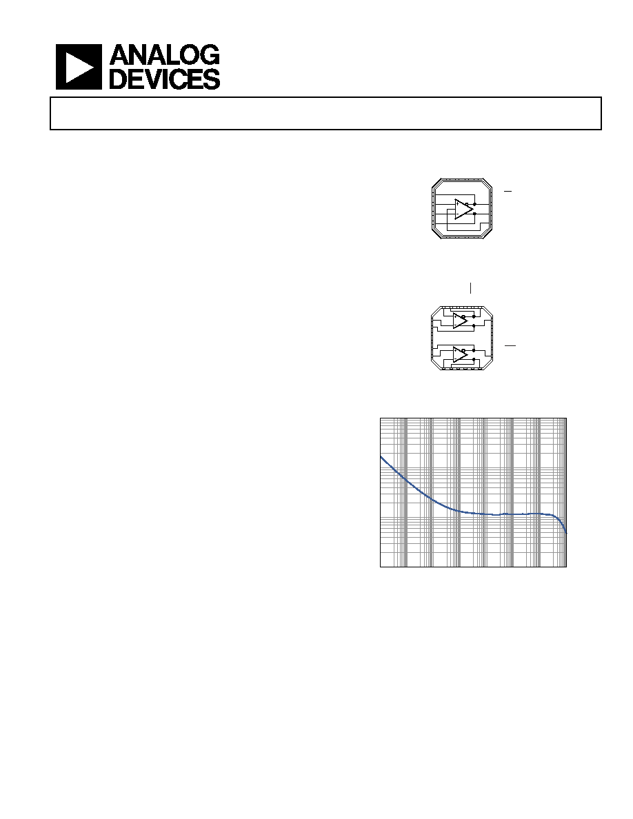
FUNCTIONAL BLOCK DIAGRAMS
1
–FB
2
+IN
3
–IN
4
+FB
11 –OUT
12 PD
10 +OUT
9VOCM
5
+
V
S
6
+
V
S
7
+
V
S
8
+
V
S
15
–V
S
16
–V
S
14
–V
S
13
–V
S
ADA4930-1
09
209-
001
Figure 1.
ADA4930-2
1
–IN1
2
+FB1
3
+VS1
4
+VS1
5
–FB2
6
+IN2
15 –VS2
16 –VS2
17 VOCM1
18 +OUT1
14 PD2
13 –OUT2
7
–I
N
2
8
+
F
B
2
9
+
V
S
2
11
V
O
C
M
2
12
+
O
U
T
2
10
+
V
S
2
21
–V
S
1
22
–V
S
1
23
–F
B
1
24
+
IN
1
20
P
D
1
19
–O
U
T
1
09
20
9-
0
02
Figure 2.
0
1
10
100
10
100
1k
10k
100k
1M
10M
100M
V
N
(nV/
√hz
)
FREQUENCY (Hz)
09
20
9-
0
03
Figure 3. Voltage Noise Spectral Density
The low dc offset and excellent dynamic performance of the
ADA4930-1/ADA4930-2 make them well suited for a wide
variety of data acquisition and signal processing applications.
The ADA4930-1 is available in a Pb-free, 3 mm × 3 mm 16-lead
LFCSP, and the ADA4930-2 is available in a Pb-free, 4 mm × 4 mm
24-lead LFCSP. The pinout has been optimized to facilitate printed
circuit board (PCB) layout and minimize distortion. The ADA4930-1
is specified to operate over the 40°C to +105°C temperature range,
and the ADA4930-2 is specified to operate over the 40°C to +105°C
temperature range for 3.3 V or 5 V supply voltages.
相关PDF资料 |
PDF描述 |
|---|---|
| 0034.5617.22 | FUSE 1A 250V T-LAG 5X20 SMD T/R |
| KTR10EZPF1804 | RES 1.80M OHM 1/8W 1% 0805 SMD |
| 0034.5619.22 | FUSE 1.6MA 250V TLAG 5X20 SMD TR |
| 0034.5615.22 | FUSE 630MA 250V TLAG 5X20 SMD TR |
| 0034.5609.22 | FUSE 160MA 250V TLAG 5X20 SMD TR |
相关代理商/技术参数 |
参数描述 |
|---|---|
| ADA4930-2YCPZ-R7 | 制造商:Analog Devices 功能描述:SP Amp DIFF AMP Dual 5.5V 24-Pin LFCSP EP T/R 制造商:Analog Devices 功能描述:ULTRALOW NOISE DRIVER FOR LOW VOLT ADC - Tape and Reel 制造商:Analog Devices 功能描述:IC DIFF AMP 1.35GHZ 24-LFCSP 制造商:Analog Devices 功能描述:IC DIFF AMP 1.35GHz 3400V/ us LFCSP- 制造商:Analog Devices 功能描述:IC, DIFF AMP, 1.35GHz, 3400V/ us, LFCSP- 制造商:Analog Devices Inc. 功能描述:Differential Amplifiers UltraLow Noise Driver for Low Volt ADC 制造商:Analog Devices 功能描述:IC, DIFF AMP, 1.35GHz, 3400V/ us, LFCSP-24; No. of Amplifiers:2; Input Offset Voltage:500V; Bandwidth:1.35GHz; Amplifier Case Style:LFCSP; No. of Pins:24; Supply Voltage Range:3.3V to 5V; Slew Rate:3400V/s; Supply Current:34mA ;RoHS Compliant: Yes 制造商:Analog Devices 功能描述:Ultralow Noise Driver for ADCs LFCSP24 |
| ADA4930-2YCPZ-R7_PROMO | 制造商:Analog Devices 功能描述:IC DIFF AMP 1.35GHZ 3400V/U |
| ADA4930-2YCPZ-RL | 功能描述:差分放大器 UltraLow Noise Driver for Low Volt ADC RoHS:否 制造商:Analog Devices 通道数量:1 Channel 带宽:900 MHz 可用增益调整:5.6 dB to 20 dB 输入补偿电压:1 mV at 5 V 共模抑制比(最小值):67 dB 工作电源电压:11 V 电源电流:28 mA 最大工作温度:+ 85 C 最小工作温度:- 40 C 安装风格:SMD/SMT 封装 / 箱体:SOIC-8 封装:Reel |
| ADA4932-1 | 制造商:AD 制造商全称:Analog Devices 功能描述:Low Power Differential ADC Driver |
| ADA4932-1_09 | 制造商:AD 制造商全称:Analog Devices 功能描述:Low Power Differential ADC Driver |
发布紧急采购,3分钟左右您将得到回复。