- 您现在的位置:买卖IC网 > PDF目录5369 > ADA4930-2YCPZ-R2 (Analog Devices Inc)IC DIFF AMP 1.35GHZ 24-LFCSP PDF资料下载
参数资料
| 型号: | ADA4930-2YCPZ-R2 |
| 厂商: | Analog Devices Inc |
| 文件页数: | 11/29页 |
| 文件大小: | 0K |
| 描述: | IC DIFF AMP 1.35GHZ 24-LFCSP |
| 标准包装: | 1 |
| 放大器类型: | 差分 |
| 电路数: | 2 |
| 输出类型: | 差分 |
| 转换速率: | 3400 V/µs |
| -3db带宽: | 1.35GHz |
| 电流 - 输入偏压: | 23µA |
| 电压 - 输入偏移: | 150µV |
| 电流 - 电源: | 34mA |
| 电流 - 输出 / 通道: | 30mA |
| 电压 - 电源,单路/双路(±): | 3.3V,5V |
| 工作温度: | -40°C ~ 105°C |
| 安装类型: | 表面贴装 |
| 封装/外壳: | 24-VFQFN 裸露焊盘,CSP |
| 供应商设备封装: | 24-LFCSP-VQ(4x4) |
| 包装: | 标准包装 |
| 其它名称: | ADA4930-2YCPZ-R2DKR |
第1页第2页第3页第4页第5页第6页第7页第8页第9页第10页当前第11页第12页第13页第14页第15页第16页第17页第18页第19页第20页第21页第22页第23页第24页第25页第26页第27页第28页第29页
ADA4930-1/ADA4930-2
Rev. A | Page 18 of 28
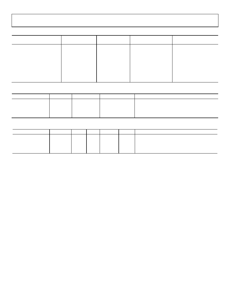
Table 11. Output Noise Voltage Density Calculations for Matched Feedback Networks
Input Noise Contribution
Input Noise Term
Input Noise
Voltage Density
Output
Multiplication Factor
Differential Output Noise
Voltage Density Terms
Differential Input
vnIN
GN
vnOD1 = GN(vnIN)
Inverting Input
inIN+
inIN+ × (RF2)
1
vnOD2 = (inIN+)(RF2)
Noninverting Input
inIN
inIN × (RF1)
1
vnOD3 = (inIN)(RF1)
VOCM Input
vnCM
0
vnOD4 = 0
Gain Resistor RG1
vnRG1
(4kTRG1)1/2
RF1/RG1
vnOD5 = (RF1/RG1)(4kTRG1)1/2
Gain Resistor RG2
vnRG2
(4kTRG2)1/2
RF2/RG2
vnOD6 = (RF2/RG2)(4kTRG2)1/2
Feedback Resistor RF1
vnRF1
(4kTRF1)1/2
1
vnOD7 = (4kTRF1)1/2
Feedback Resistor RF2
vnRF2
(4kTRF2)1/2
1
vnOD8 = (4kTRF2)1/2
Table 12. Differential Input, DC-Coupled, VS = 5 V
Nominal Gain (dB)
RF1, RF2 (Ω)
RG1, RG2 (Ω)
RIN, dm (Ω)
Differential Output Noise Density (nV/√Hz)
0
301
602
4.9
6
301
150
300
6.2
10
301
95.3
190.6
7.8
14
301
60.4
120.4
10.1
Table 13. Single-Ended Ground-Referenced Input, DC-Coupled, RS = 50 Ω, VS = 5 V
Nominal Gain (dB)
RF1, RF2 (Ω)
RG1 (Ω)
RT (Ω)
RIN, cm (Ω)
Differential Output Noise Density (nV/√Hz)
0
301
142
64.2
190.67
170
5.9
6
301
63.4
84.5
95.06
95
7.8
10
301
33.2
1 k
53.54
69.3
9.3
14
301
10.2
1.15 k
17.5
57.7
10.4
1 RG2 = RG1 + (RS||RT).
Table 11 summarizes the input noise sources, the multiplication
factors, and the output-referred noise density terms.
Table 12 and Table 13 list several common gain settings, associated
resistor values, input impedance, and output noise density for
both balanced and unbalanced input configurations.
IMPACT OF MISMATCHES IN THE FEEDBACK
NETWORKS
As previously mentioned, even if the external feedback networks
(RF/RG) are mismatched, the internal common-mode feedback
loop still forces the outputs to remain balanced. The amplitudes
of the signals at each output remain equal and 180° out of phase.
The input-to-output differential mode gain varies proportionately
to the feedback mismatch, but the output balance is unaffected.
The gain from the VOCM pin to VO, dm is equal to
2(β1 β2)/(β1 + β2)
When β1 = β2, this term goes to zero and there is no differential
output voltage due to the voltage on the VOCM input (including
noise). The extreme case occurs when one loop is open and the
other has 100% feedback; in this case, the gain from VOCM input
to VO,dm is either +2 or 2, depending on which loop is closed. The
feedback loops are nominally matched to within 1% in most
applications, and the output noise and offsets due to the VOCM
input are negligible. If the loops are intentionally mismatched by a
large amount, it is necessary to include the gain term from VOCM
to VO, dm and account for the extra noise. For example, if β1 = 0.5
and β2 = 0.25, the gain from VOCM to VO, dm is 0.67. If the VOCM pin
is set to 0.9 V, a differential offset voltage is present at the output of
(0.9 V)(0.67) = 0.6 V. The differential output noise contribution is
(5 nV/√Hz)(0.67) = 3.35 nV/√Hz. Both of these results are
undesirable in most applications; therefore, it is best to use
nominally matched feedback factors.
Mismatched feedback networks also result in a degradation of
the ability of the circuit to reject input common-mode signals,
much the same as for a four-resistor difference amplifier made
from a conventional op amp.
As a practical summarization of the previous issues, resistors of
1% tolerance produce a worst-case input CMRR of approximately
40 dB, a worst-case differential-mode output offset of 9 mV due
to a 0.9 V VOCM input, negligible VOCM noise contribution, and
no significant degradation in output balance error.
INPUT COMMON-MODE VOLTAGE RANGE
The input common-mode range at the summing nodes of the
ADA4930-1/ADA4930-2 is specified as 0.3 V to 1.5 V at VS = 3.3 V.
To avoid nonlinearities, the voltage swing at the +IN and IN
terminals must be confined to these ranges.
相关PDF资料 |
PDF描述 |
|---|---|
| 0034.5617.22 | FUSE 1A 250V T-LAG 5X20 SMD T/R |
| KTR10EZPF1804 | RES 1.80M OHM 1/8W 1% 0805 SMD |
| 0034.5619.22 | FUSE 1.6MA 250V TLAG 5X20 SMD TR |
| 0034.5615.22 | FUSE 630MA 250V TLAG 5X20 SMD TR |
| 0034.5609.22 | FUSE 160MA 250V TLAG 5X20 SMD TR |
相关代理商/技术参数 |
参数描述 |
|---|---|
| ADA4930-2YCPZ-R7 | 制造商:Analog Devices 功能描述:SP Amp DIFF AMP Dual 5.5V 24-Pin LFCSP EP T/R 制造商:Analog Devices 功能描述:ULTRALOW NOISE DRIVER FOR LOW VOLT ADC - Tape and Reel 制造商:Analog Devices 功能描述:IC DIFF AMP 1.35GHZ 24-LFCSP 制造商:Analog Devices 功能描述:IC DIFF AMP 1.35GHz 3400V/ us LFCSP- 制造商:Analog Devices 功能描述:IC, DIFF AMP, 1.35GHz, 3400V/ us, LFCSP- 制造商:Analog Devices Inc. 功能描述:Differential Amplifiers UltraLow Noise Driver for Low Volt ADC 制造商:Analog Devices 功能描述:IC, DIFF AMP, 1.35GHz, 3400V/ us, LFCSP-24; No. of Amplifiers:2; Input Offset Voltage:500V; Bandwidth:1.35GHz; Amplifier Case Style:LFCSP; No. of Pins:24; Supply Voltage Range:3.3V to 5V; Slew Rate:3400V/s; Supply Current:34mA ;RoHS Compliant: Yes 制造商:Analog Devices 功能描述:Ultralow Noise Driver for ADCs LFCSP24 |
| ADA4930-2YCPZ-R7_PROMO | 制造商:Analog Devices 功能描述:IC DIFF AMP 1.35GHZ 3400V/U |
| ADA4930-2YCPZ-RL | 功能描述:差分放大器 UltraLow Noise Driver for Low Volt ADC RoHS:否 制造商:Analog Devices 通道数量:1 Channel 带宽:900 MHz 可用增益调整:5.6 dB to 20 dB 输入补偿电压:1 mV at 5 V 共模抑制比(最小值):67 dB 工作电源电压:11 V 电源电流:28 mA 最大工作温度:+ 85 C 最小工作温度:- 40 C 安装风格:SMD/SMT 封装 / 箱体:SOIC-8 封装:Reel |
| ADA4932-1 | 制造商:AD 制造商全称:Analog Devices 功能描述:Low Power Differential ADC Driver |
| ADA4932-1_09 | 制造商:AD 制造商全称:Analog Devices 功能描述:Low Power Differential ADC Driver |
发布紧急采购,3分钟左右您将得到回复。